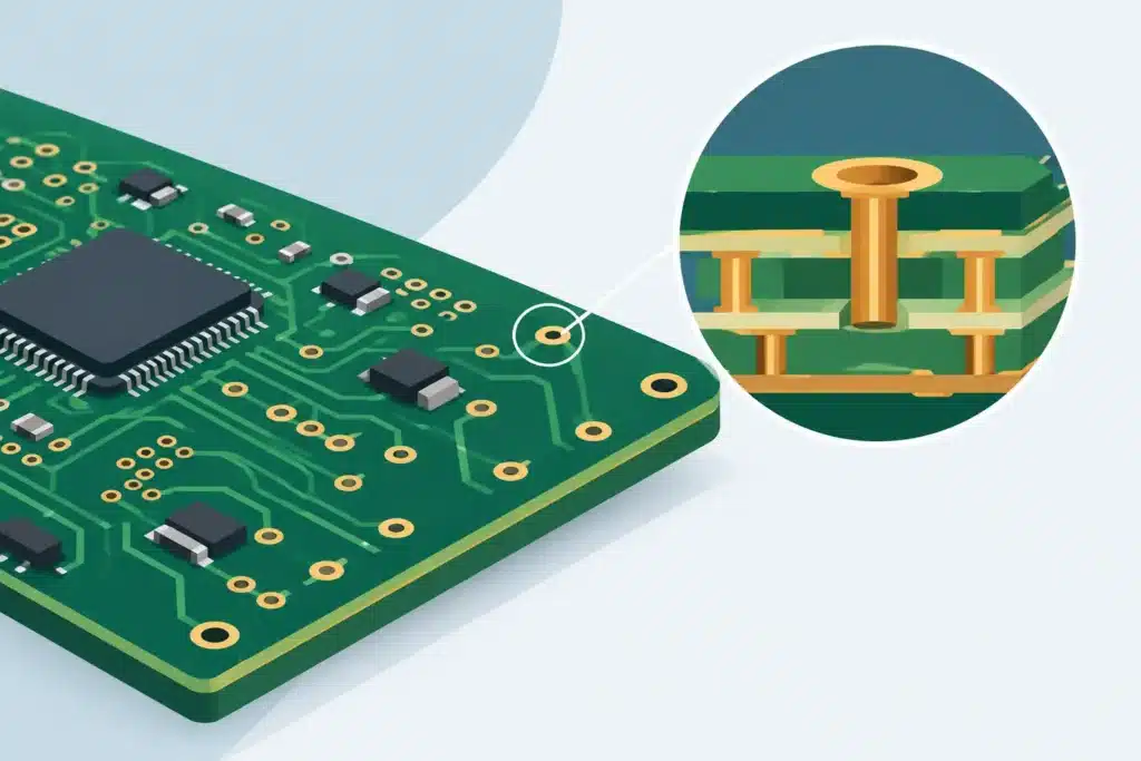
A differential bus specified for 100 ohms does not become 100 ohms simply because the trace is routed with a specific width. PCB impedance calculation depends on the entire physical construction: layer stackup, dielectric properties, copper thickness, reference planes, solder mask, trace width, trace spacing, and, critically, the manufacturer’s actual material data. If even one of these parameters changes, the impedance changes as well.
This is critical in designs featuring high data rates, fast edge rates, RF, precision clock signals, and sensitive analog circuits. Here, controlled impedance is not a cosmetic specification in the layout documentation. It is a fundamental prerequisite for signal integrity, EMC performance, and reliable operation in the final hardware.
Why Impedance Calculation Must Start with the Stackup
The most common mistake is defining trace width first and the stackup later. In practice, the sequence must be reversed. An impedance value can only be calculated meaningfully based on a specific stackup agreed upon with the selected PCB manufacturer.
For a microstrip on an outer layer, the distance to the reference plane, the material's dielectric constant, the copper thickness, and potentially the solder mask are critical parameters. For a stripline routed between two planes, there is additional dependency on the distance to both planes and whether the trace is positioned symmetrically within the dielectric. With differential routing, the coupling between the two conductors must also be factored in.
A generic four-layer PCB specified merely with "FR-4" is therefore insufficient as a design baseline. FR-4 is a material category, not a single, unambiguous dielectric constant. Dk varies with laminate type, glass weave style, resin content, frequency, and the manufacturer's test methodology. For standard digital interfaces, this variation may be manageable if tolerances are appropriately defined. For RF, SerDes, and ultra-high-speed interfaces, it must be evaluated explicitly.
A calculation is only valuable when it accurately models a manufacturable construction. Therefore, the stackup should include nominal and relevant tolerance values for pressed prepreg thickness, core thicknesses, copper weights, material families, and reference planes. Without this foundation, routing risks being optimized based on assumptions rather than manufacturing reality.
PCB Impedance Calculation: The Critical Inputs
An impedance calculator can provide a number in seconds. The engineering challenge lies in determining whether the input data is accurate and whether the result is manufacturable within the specified tolerance.
For single-ended signals, characteristic impedance is often specified at 50 ohms, for example, while differential pairs are typically specified at 90, 100, or 110 ohms differentially, depending on the interface and standard. It is essential to distinguish between differential impedance and the single-ended impedance of each trace. A 100-ohm differential pair does not inherently consist of two arbitrary 50-ohm traces. The spacing between them alters the electromagnetic coupling and, consequently, the total differential impedance.
The primary input parameters are trace width, copper thickness, height above the reference plane, dielectric constant, and trace spacing. However, several critical factors are frequently overlooked:
- Etching alters trace geometry. A finished, etched trace typically exhibits a trapezoidal profile rather than a perfectly rectangular cross-section.
- Solder mask primarily affects outer layers and must be included in calculations when tolerances are tight.
- Glass weave can cause localized variations in effective Dk, leading to timing skew—commonly referred to as the fiber weave effect.
- Vias, pads, connector footprints, and layer transitions introduce discontinuities that simple transmission line calculations do not resolve.
- The reference plane must remain continuous. A correctly calculated trace loses its integrity if the return current is forced around a split plane or a large antipad void.
This final point is particularly critical. Impedance is not solely about the signal trace; it encompasses the signal's complete field distribution and return path. When a reference plane is disrupted, the loop area increases, introducing risks of signal reflections, common-mode noise, and elevated emissions.
Microstrip or Stripline?
The choice between microstrip and stripline involves both electrical performance and manufacturability trade-offs. Microstrip on outer layers is often easier to route, simpler to measure, and practical for connector interfaces. Conversely, the electromagnetic field is partially exposed to the environment, increasing sensitivity to solder mask variations, adjacent components, and EMI.
Stripline is shielded between reference planes and typically provides superior EMC performance. However, it demands stricter discipline regarding via transitions and breakout routing, and it may exhibit higher losses at high frequencies depending on material selection and copper roughness. There is no single correct choice. The decision depends on frequency, edge rates, layer count, routing density, EMI requirements, and overall manufacturing economics.
From Schematic Requirements to a Production-Ready Layout
Impedance control must be mapped to actual net classes across both schematic and layout. This begins by identifying signals with defined impedance requirements: RF transmission lines, USB, Ethernet, PCI Express, MIPI, LVDS, DDR clocks, SerDes lanes, and other high-speed or timing-critical interfaces.
Next, the layer stackup strategy is defined. Critical signals are routed on layers with continuous reference planes, utilizing geometries that align realistically with manufacturer process capabilities. Extremely narrow traces and ultra-tight gaps may be theoretically correct in calculations, but they rarely represent an optimal solution if they push etch tolerances, layer registration, or yield to their limits.
A robust design maintains margin. If a 100-ohm differential pair can only be achieved via an extremely sensitive combination of a 75 µm trace and a 75 µm gap, the stackup or layer allocation should be re-evaluated. Increasing the dielectric height, selecting an alternative copper layer, or choosing a laminate with tighter material specifications can yield a geometry that is both more stable and easier to manufacture.
Furthermore, impedance specifications should not be considered in isolation. Length matching, skew budgets, insertion loss, via stubs, and connector transitions can be equally decisive. On a 25 Gbps channel, a pristine 100-ohm trace will still fail if stubs and transition geometries remain unmanaged. In RF designs, a short trace referencing the wrong plane or an uncharacterized via inductance can shift impedance matching significantly.
Tolerances Are Part of the Specification
Specifying "50 ohms" on a fabrication drawing is insufficient. The requirement must state the target value, tolerance, applicable layers, and whether the measurement applies to single-ended or differential impedance. The specified tolerance must be technically justified; tighter tolerances are not inherently better if variations across the components and the broader channel are considerably larger.
For many digital designs, a practical tolerance of ±10 percent is both realistic and functionally robust. Other applications require ±7 or ±5 percent, but this must be aligned with manufacturer capabilities, material selection, and testing methodologies. A specification that cannot be validated in production provides a false sense of security.
Impedance coupons are therefore essential when tight control is required. A test coupon is manufactured alongside the panel and typically verified using TDR (Time-Domain Reflectometry). The result validates the fabricated geometry, but it does not replace comprehensive design verification. The coupon represents a controlled test structure—not necessarily all critical transitions and discontinuities present on the actual board.
Simulation Complements Calculation
A 2D field solver is ideal for establishing trace geometries on a defined stackup. It models the cross-section and provides a reliable baseline for controlled impedance routing rules. However, when geometries transition into three dimensions, more advanced analysis is required.
BGA breakouts, layer transitions via stubs, backdrilling, connector launches, RF transitions, and plane cutouts must be analyzed as 3D structures. In these scenarios, 3D electromagnetic simulation or dedicated SI analysis becomes necessary. This is especially true when failures only surface late in the hardware lifecycle—manifesting as overshoot, eye closure, emissions compliance issues, or unexpected sensitivity to cables and temperature variations.
The most cost-effective approach is front-loading analysis early in the design cycle. It is substantially cheaper to optimize stackup and routing rules prior to layout sign-off than to execute redesign iterations following EMC compliance testing or initial prototype bring-up.
Common Pitfalls That Drive Costly Iterations
The first pitfall is copying routing rules directly from a previous design. Even if the interface and manufacturer remain identical, differences in layer stackup or copper weight can render the legacy geometry invalid.
The second is routing a differential pair with constant center-to-center pitch without accounting for how component fanout, pads, and vias alter coupling. It is often necessary to manage both trace width and spacing through critical zones, rather than focusing solely on the uninterrupted run between components.
The third is neglecting the return current path during layer transitions. When a signal changes reference planes, the return current requires a low-inductance path between the planes. For differential pairs, properly placed stitching vias may be essential. Omitting them can create severe EMC issues, even if the nominal trace impedance remains strictly within tolerance.
The fourth is treating the fabricator's stackup as a late-stage procurement detail. In advanced PCB design, the stackup is an electrical specification. It must be finalized collaboratively with manufacturing while there is still freedom to adjust layer assignments, materials, and geometries.
Impedance Must Hold True Through to Final Measurement
Accurate impedance control is not a single value derived from a basic calculator. It is an integrated engineering process that extends from interface requirements and stackup design to routing constraints, fabrication data, test coupons, and physical verification. When executed with technical discipline, this process mitigates reflections, jitter, EMC compliance failures, and costly board revisions.
For complex printed circuit boards, the question is never simply whether a trace "looks right." The question is whether the entire signal path is validated against the actual stackup and fabrication processes deployed on the factory floor. That is where impedance calculations provide genuine engineering value—ensuring a board operates reliably and without guesswork.