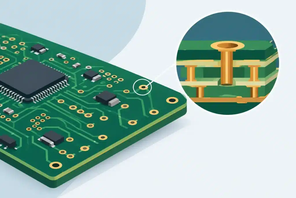
An EMC failure rarely manifests where its root cause originates. A non-compliance peak at 180 MHz may be driven by a switch-mode power supply, a cable carrying common-mode current, or a disrupted return current path far from the component initially suspected. Troubleshooting EMC issues should therefore not begin by scattering ferrites at random. It must begin with a technical explanation of how the noise is generated, where it couples, and the path it takes to exit the product.
For engineering teams across industrial, medical, telecommunications, and defense sectors, a failed EMC test is more than just a test laboratory result. It can block product release, trigger costly layout revisions, and introduce uncertainty into a platform otherwise ready for production. The fastest path forward is a disciplined methodology where measurement data, PCB geometry, the PDN, and the system's mechanical construction are evaluated holistically.
Start by Distinguishing Between Emissions and Immunity
EMC encompasses two fundamental domains. Emissions concern what the product itself radiates or conducts into its environment. Immunity addresses what the product can withstand from external phenomena—such as ESD, EFT/burst, surge, or RF fields. While the symptoms may appear similar, the diagnostic methodologies differ significantly.
In emissions troubleshooting, the task typically involves identifying the noise source, the coupling mechanism transferring the energy, and the antenna structure or cabling effectively radiating it. In immunity, the focus shifts to entry paths for external energy and why an interface, a reset trace, or a power rail loses its noise margin. A product can easily pass emissions testing and still fail immunity drastically. Consequently, resolving both domains with an identical component modification is rarely effective.
Frequency provides a critical diagnostic trail. A narrow, periodic peak typically points to a clock, a DC/DC regulator, or a harmonic from a periodic switching function. A broader noise spectrum may stem from fast edge rates, ringing, inadequate decoupling, or multiple concurrent noise sources. However, frequency alone is not definitive proof; it must be correlated with circuit timing, cable geometry, and the operating modes under which the failure occurs.
Troubleshooting EMC Issues Requires a Measurable Baseline
A test report from an accredited laboratory is valuable, but it generally only indicates that limits were exceeded at specific frequencies and measurement setups. Before modifying hardware, the failure must be reproducible internally or within a pre-compliance test environment. Otherwise, every mitigation or degradation remains mere guesswork.
Therefore, lock down the product configuration: firmware release, active interfaces, load conditions, cable types, cable routing, power supply, chassis grounding state, and temperature. An Ethernet port operating under full traffic, an active motor drive, or a specific data rate can alter the EMC profile substantially. Isolating a failure to a single operating state provides the most actionable constraint for the engineering team.
Near-field probes, a spectrum analyzer, and RF current probes are indispensable tools during the initial phase. They enable localized comparisons across the PCB, current measurements on individual cables, and immediate verification of whether an intervention shifts a peak. The measurement does not need to achieve full normative compliance on day one; it must be sufficiently stable to differentiate true signal behavior from measurement variance.
A systematic workflow entails:
- Confirm the critical frequency and operational mode.
- Map whether energy is most prominent at the noise source, along the return plane, at the connector, or on the cable harness.
- Modify a single physical parameter at a time and re-measure.
- Document the quantitative effect, secondary side effects, and the technical rationale.
This methodology may seem slower than testing multiple filter topologies simultaneously. In practice, it accelerates resolution because the engineering team maintains clear causality and prevents the introduction of secondary signal integrity, thermal, or manufacturing defects.
Identify the Source, Coupling Path, and Antenna
An EMC failure can typically be broken down into three elements: the source, the coupling path, and the antenna. The source may be a clock driver, a switching node, a differential driver, or a high dI/dt transient. The coupling mechanism may be capacitive, inductive, conducted, or common-mode. The antenna may be an external cable, a chassis aperture, an inadequately terminated shield plane, or an excessively large loop on the PCB.
Addressing the wrong element yields negligible results. If an unfiltered cable acts as the radiating antenna, marginally attenuating switching ripple at the regulator will provide limited benefit. If common-mode current is induced by skew or asymmetry in a high-speed differential interface, increasing bulk capacitance on the power rail is irrelevant.
Return current paths are frequently the overlooked variable. High-frequency currents do not follow the path of least resistance, but rather the path of least impedance—typically running directly adjacent to the signal trace and its reference plane. When a signal traverses a split, a cutout, a layer transition lacking sufficient stitching vias, or an interrupted reference plane, the return current is forced into a detour. This expands loop area, escalates radiation, and increases cross-coupling into adjacent nets.
Connectors demand identical scrutiny. A cable interface must be treated as a transition between the PCB, the mechanical chassis, and the external environment. Filter components placed centimeters away from the connector leave an unshielded PCB trace that continues to couple noise onto the cable. Shield termination, chassis grounding, and common-mode choke placement must therefore be evaluated as an integrated structure, rather than isolated schematic symbols.
Switch-Mode Power Supplies: Frequent Suspects, but Not Always the Cause
DC/DC converters are often the primary suspects because their switch nodes exhibit high dV/dt, generating pronounced harmonic content. While scrutinizing them is sound practice, the mitigation depends strictly on layout geometry. A compact hot loop, minimal trace inductance between the input capacitor and switching elements, and a tightly controlled return path reduce both electric fields and magnetic loop area.
If ringing is the dominant mechanism, gate resistors, RC snubbers, or alternative component selections may be warranted. However, every modification incurs trade-offs. Slower edge rates increase switching losses and thermal dissipation, whereas a snubber may improve EMC margins at the expense of conversion efficiency and component derating. Any layout or BOM modification must be validated against EMC, thermal performance, and dynamic load variations.
Treat High-Speed Signals as Transmission Lines
USB, Ethernet, PCIe, LVDS, and high-speed memory buses can induce severe EMC failures even when passing standard functional validation. Controlled impedance, precise differential pair geometry, minimal stub lengths, and continuous reference planes are critical. A via stub or asymmetry in a differential routing transition converts differential-mode energy into common-mode energy, which readily propagates onto cabling or enclosure structures.
In these scenarios, an implementation that appears clean in a CAD layout viewer may prove electrically inadequate. Stackup design, dielectric characteristics, copper roughness, reference transitions, and connector footprint breakout all participate in the same high-frequency network. At marginal frequencies, physical measurements should be augmented with signal integrity and PDN simulations rather than relying solely on empirical trial and error.
Avoid Symptomatic Mitigations Using Ferrites and Ad-Hoc Capacitors
Ferrite beads, common-mode chokes, feedthrough capacitors, and shielding cans are standard EMC mitigation tools. Issues arise when they are applied indiscriminately without detailed analysis of frequency range, current profiles, and return paths. A ferrite bead may provide high impedance in a narrow band while exhibiting poor attenuation at the critical harmonic. It can also induce DC voltage drop or compromise supply rail stability during load transients.
Similarly, adding decoupling capacitors may suppress local voltage ripple without resolving radiated emissions. The component's mounting inductance (ESL), routing geometry to the planes, and interaction with the wider PDN dictate its efficacy. Scattering capacitors without a planned impedance profile merely increases BOM cost and assembly complexity without delivering measurable EMC margin.
An effective countermeasure must address the verified physical mechanism. This may involve restoring reference continuity, relocating an I/O connector, reconfiguring the layer stackup, optimizing chassis bonding, or defining a dedicated filter zone. Component-level adjustments are the final stage of the solution, not a substitute for electromagnetic fundamentals.
Integrate EMC as a Design Parameter Prior to Compliance Testing
The most cost-effective EMC failure to resolve is the one eliminated before the first prototype run. This requires integrating EMC analysis into design reviews alongside DFM, thermal analysis, and signal integrity. Critical nets, connectors, cable routings, switching loops, and chassis ground references must be scrutinized explicitly—not discovered during final certification testing.
In complex PCBs, the layer stackup and component placement must be established with EMC constraints defined before trace routing is locked down. Requirements include continuous reference planes, clear domain isolation between noisy and sensitive circuits, defined return current paths at layer transitions, and adequate space for filtering directly at interface boundaries. While HDI technology provides greater flexibility, its advantages depend entirely on the deliberate use of microvias, buildup layers, and reference transitions.
Wise Choice Support bridges the gap between schematic intent, PCB layout, and verifiable EMC performance, ensuring modifications are not restricted to symptomatic fixes. During a critical design review, our objective is not to impose arbitrary guidelines, but to identify precise layout, current-return, or interface vulnerabilities that compromise compliance margins.
When an EMC issue arises, the optimal response is not an immediate component order. It is a controlled measurement that isolates the physical mechanism and guides a design revision that can be reliably manufactured in volume.