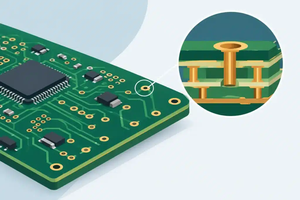
A BGA package with a 0.5 mm pitch, multiple DDR lines, and a compact mechanical enclosure can quickly make a traditional multilayer PCB unfeasible. The question of when to use HDI PCBs is therefore not about selecting the most advanced technology, but about choosing the build-up that can be routed, manufactured, and operate reliably throughout the product's lifecycle.
HDI stands for High Density Interconnect. The technology typically utilizes laser-drilled microvias, blind and buried vias, and sequential layer build-up. This provides significantly more routing options in close proximity to components than through-hole plated vias alone. The benefits can be decisive, but they come with stricter requirements for layout, stackup, material selection, DFM, and manufacturer process control.
When is there a Justified Need for HDI PCBs?
HDI becomes relevant when routing cannot be practically achieved on a conventional board without unreasonably increasing layer count, board dimensions, or manufacturing risk. This is particularly prevalent in products where high component density is combined with fine-pitch packages, high data rates, or tight mechanical constraints.
The most common trigger is component breakout. A fine-pitch BGA does not necessarily leave sufficient space for traditional via dog-bones between pads. Utilizing via-in-pad and laser-drilled microvias allows signals to drop directly from the pad into the next layer. This frees up surface routing space and enables escape routing for more nets without forcing trace width and spacing below limits that PCB fabricators can reliably produce with stable yields.
HDI is also essential when the board must be smaller or thinner without compromising functionality. Examples include compact RF units, advanced sensor modules, medical devices, and embedded computing systems. In these applications, increasing component pitch or adding more through-hole vias is rarely a viable option, as mechanical constraints, enclosures, and thermal management strategies are already fixed.
In data center, telecommunications, and radar equipment, HDI can also serve as part of the solution surrounding processors, FPGAs, memory, and high-speed interfaces. However, it is critical to distinguish between the need for high density and the need for high-speed signal performance. HDI does not inherently resolve signal integrity issues. On the contrary, it can introduce new requirements for reference planes, via transitions, impedance control, and return paths.
Technical Indicators that Standard Technology is Insufficient
A layout should be evaluated based on concrete constraints—not on a general assumption that HDI is inherently superior. The initial assessment is whether critical components can be escaped using the desired padstack, trace widths, and clearances realistic for the selected manufacturing process.
If a BGA requires more routing channels than can be established between solder balls and on adjacent layers, HDI is often the appropriate next step. The same applies if through-hole vias consume so much internal layer area that power planes become heavily perforated, or high-speed traces are forced into excessively long and convoluted routing topologies.
For DDR, PCI Express, Ethernet, SerDes, and RF interconnects, evaluation must extend beyond basic breakout. A dense design still requires continuous reference planes, controlled impedance, and a clearly defined return path at every layer transition. Microvias can minimize via stubs and shorten the transition between component and transmission line. This can improve electrical performance, but only if the stackup and via geometry are specifically engineered for the target signal speeds.
PDN performance is another critical factor. Fine-pitch BGAs frequently incorporate extensive power and ground pin counts that must be accommodated without introducing copper distribution bottlenecks. HDI can provide improved access to power and ground directly beneath the component, yet sufficient area must remain reserved for planes, decoupling capacitors, and adequate copper volume for current capacity and thermal dissipation. A denser layout must never compromise power integrity.
HDI is Not Always the Right Solution
A design with high pin counts does not automatically require HDI. In many cases, a marginally larger PCB form factor, a BGA with a coarser pitch, or two additional conventional layers provides the most reliable and cost-effective approach. This is particularly true for moderate production volumes, where engineering and fabrication costs must be evaluated holistically.
A conventional stackup with through-hole vias may also be preferred if the design involves high current demands, heavy copper weights, or specialized dielectric isolation requirements. HDI builds typically utilize thinner dielectrics and more complex fabrication cycles. This imposes higher demands on thermal management, copper balance, and warpage control.
For high-speed signals, backdrilling conventional through-hole vias can sometimes represent a simpler alternative to a comprehensive HDI architecture. Backdrilling eliminates a significant portion of the via stub while retaining a more conventional board construction. The optimal choice depends on frequency content, layer count, component placement, volume, and the specific board fabricator's process capabilities.
Pushing trace width and spacing to absolute minimum limits is not always advisable either. Extremely fine geometries may appear favorable in CAD layouts, but they can degrade fabrication yields and severely restrict supplier options. The optimal approach consistently achieves electrical and mechanical targets with robust process margins.
Define the HDI Architecture Before Routing Freezes
HDI must be planned as a core element of the initial design framework. Postponing this decision until layout completion risks requiring extensive rework of component placement, stackup design, impedance calculations, and critical routing. The costly mistake is rarely the microvia itself; it is discovering too late that the selected via structure cannot be reliably manufactured or fails to support an electrically sound topology.
A typical HDI configuration may employ a 1+N+1 build-up, featuring a single sequential lamination layer on each side of a conventional core. This is frequently sufficient to escape components with moderately fine pitches. More compact designs may dictate a 2+N+2 or higher sequential build-up. Each additional lamination cycle expands design flexibility, but correspondingly increases manufacturing complexity, lead times, and documentation requirements.
The selection between staggered and stacked microvias is equally critical. Staggered vias are typically simpler to fabricate and yield a more conservative, reliable interconnect. Stacked vias conserve valuable surface area but require precise copper filling, planarization, and tight process controls. For hardware exposed to thermal cycling, vibration, or extended operating life profiles, this trade-off must be evaluated against fabricator capabilities and reliability standards.
Manufacturing and Reliability Must Inform the Decision
An HDI board design is not complete simply because it routes successfully. Gerber or ODB++ data must reliably translate into a consistent, yield-stable product at the chosen production facility. Fabrication drawings, stackup definitions, material specifications, drill tables, impedance targets, and acceptance criteria must be rigorously defined and aligned.
Via-in-pad implementations, for instance, typically necessitate filled and planarized vias to prevent solder migration during assembly. This impacts both fabrication costs and process flow. Microvias must also be dimensioned in accordance with the manufacturer's verified laser ablation, plating, and via-fill capabilities. Generic design rules are insufficient when hardware must be reliably produced across multiple production runs or qualified secondary sources.
For IPC Class 3 designs, aerospace, defense, and critical medical systems, thermomechanical stress requires rigorous scrutiny. Microvia profiles, copper fill integrity, layer thicknesses, and dielectric Z-axis expansion characteristics directly govern how the assembly withstands reflow cycles, operational thermal shifts, and mechanical stress. The objective is not an arbitrary proliferation of design constraints, but a fully documented build backed by appropriate reliability margins.
A Practical Decision Framework for HDI
The soundest architectural decisions result from evaluating electrical, mechanical, and fabrication requirements concurrently. Begin with component pitch, pin counts, and breakout requirements. Next, establish the required layer allocation for signals, reference planes, power distribution, and thermal relief. Only then is it appropriate to define the via architecture and verify whether a conventional stackup remains feasible.
Critical nets must be simulated and verified against the actual stackup definition. This analysis includes characteristic impedance, insertion loss, via transitions, crosstalk, and PDN performance. Concurrently, component placement must be evaluated relative to decoupling efficiency, thermal management, assembly clearances, and EMC compliance. An HDI implementation that merely optimizes component breakout at the expense of power delivery integrity or clean return paths provides no technical benefit.
Subsequently, fabricator DFM feedback must be integrated before finalizing the layout. Key parameters include minimum annular rings, microvia dimensions, aspect ratios, via fill integrity, copper weights, and manufacturing tolerances. Wise Choice Support integrates these verifications early in the development cycle, ensuring that production-ready designs achieve repeatable fabrication results—far exceeding basic design rule checks.
When HDI is selected based on documented routing, signal integrity, and manufacturing requirements, it represents a precise, highly effective engineering solution. When adopted merely out of routine, it frequently introduces unnecessary production costs. The appropriate time to transition to HDI is when physical constraints demand it, and HDI provides the most predictable, reliable path to a PCB that performs robustly beyond the CAD environment.