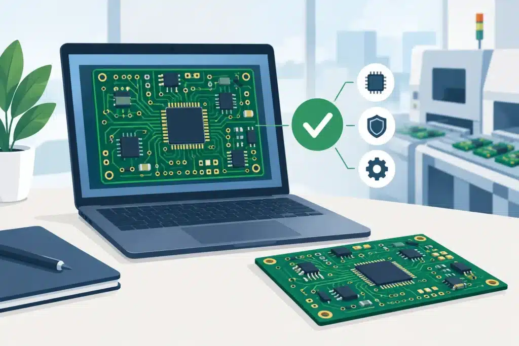
When a high-speed design fails in the EMC chamber, during temperature testing, or at the customer site, the root cause is rarely mysterious. It typically stems from an interplay among stackup, impedance, reference planes, vias, and component placement that was never evaluated holistically. A signal integrity analysis makes these dynamics quantifiable before they result in re-spins, delayed certifications, or field instability.
Signal integrity is not merely about whether a digital signal arrives at its destination. It is about whether the receiver observes the correct voltage at the correct time with adequate margin—even when the board is hot, heavily loaded, manufactured within standard process variations, and subjected to noise from the rest of the system. At high edge rates, even seemingly short interconnects behave as transmission lines. Consequently, a design with a moderate clock frequency can still demand the exact same rigor as a significantly faster interface.
When Signal Integrity Analysis Is Necessary
Analysis is critical when the design incorporates DDR memory, Ethernet, PCI Express, USB, SerDes, LVDS, MIPI, ADC/DAC interfaces, or high-speed FPGA connections. The same applies to digital circuitry adjacent to RF, where digital noise can couple into sensitive analog domains. However, the need is not determined solely by an arbitrary frequency threshold.
Edge rate, trace length, topology, and PCB manufacturing tolerances are frequently more critical than the nominal data rate. For example, a 100 MHz clock with fast rise times can generate substantial reflections on an interconnect that traditional layout guidelines would categorize as electrically short. If the physical length is significant relative to the signal's rise time, the trace is electrically long.
The analysis should be initiated when selecting components, defining pinouts, and establishing the layer stackup—not after routing is complete. While a datasheet specifies requirements for impedance, termination, and timing, it does not translate those constraints to a specific PCB layout with a defined stackup, via geometry, and manufacturing partner. It is precisely in this translation that many design failures originate.
What a Signal Integrity Analysis Actually Evaluates
The objective is to document signal behavior from driver to receiver and identify areas where margins are inadequate. The methodology integrates circuit theory, stackup parameters, layout geometries, and relevant IBIS or SPICE models. A reliable analysis is not merely a colorful simulation plot; it is founded on realistic assumptions, documented tolerances, and an engineering understanding of what the models can and cannot capture.
Impedance and Reflections
A signal experiences an impedance discontinuity at incorrect trace widths, layer transitions, vias, connectors, or stubs. A portion of the energy reflects back toward the source, potentially causing overshoot, undershoot, ringing, and multiple threshold crossings at the receiver. On an oscilloscope in a basic test setup, a signal may still appear acceptable while lacking sufficient operating margin in the final product.
Controlled impedance begins with the stackup. Dielectric thickness, copper weight, trace width, and reference planes must be established in collaboration with the PCB manufacturer. Selecting a nominal 50-ohm single-ended or 100-ohm differential rule in CAD software without a verified stackup is not controlled engineering—it is an assumption.
Return Paths and Reference Planes
High-speed signals do not simply propagate forward along the copper trace. The return current follows the path of least inductance, typically directly beneath the signal on the nearest continuous reference plane. If this plane is disrupted by a split, a cutout, or an improper layer transition, the return current is forced to detour. This increases loop area, noise, and radiated emissions.
A signal via transitioning from one layer referenced to GND to another layer referenced to GND typically requires an adjacent GND stitching via to provide a continuous return path. When a signal transitions reference between GND and a power plane, the evaluation becomes more complex. Here, the PDN impedance and inter-plane decoupling must be taken into account. Consequently, the mechanical placement of a single via can directly impact both signal integrity and EMC performance.
Timing, Jitter, and Eye Diagrams
For parallel buses, delay matching is critical; however, matched physical trace length does not equate to matched electrical propagation delay. Vias, dielectric variations across layers, copper morphology, and component pads alter the actual propagation delay. For differential pairs, both total pair delay and intra-pair skew must be evaluated.
For high-speed serial links, the eye diagram provides an effective representation of system margins. A closed or degraded eye can result from insertion loss, reflections, crosstalk, jitter, or suboptimal equalization settings. The objective is not simply to achieve an open eye diagram in isolation, but to understand the physical mechanisms causing eye closure and determine whether remediation requires changes to layout, component selection, or link configuration.
Crosstalk and Coupling
Adjacent traces couple capacitively and inductively. The risk increases with parallel routing, tight spacing, fast edge rates, and absent reference planes. Crosstalk can manifest as timing errors, elevated jitter, or noise induced onto sensitive analog nets. Conversely, applying overly conservative spacing rules across all nets increases board area, layer count, and overall manufacturing cost.
The optimal strategy is governed by net criticality. High-priority clocks, reset lines, and high-speed links must be prioritized, whereas low-speed GPIO lines can often be routed under more pragmatic rules. Design rules must reflect functional criticality and electrical risk rather than a generic spacing table applied indiscriminately across the entire layout.
From Analysis to a Production-Ready Layout
An effective analysis culminates in actionable layout decisions. These may include stackup definition, maximum stub length constraints, backdrilling requirements, AC coupling capacitor placement, series termination implementation, or revised component floorplanning. Every recommendation must trace directly to an electrical requirement and remain fully manufacturable.
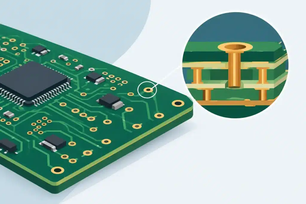
Vias represent a typical engineering trade-off. Microvias, blind vias, and backdrilling minimize stubs and optimize high-frequency performance, but they influence fabrication cost, supplier options, and production yield. On a board with moderate data rates, standard through-hole vias may be entirely adequate. For multi-gigabit SerDes interfaces, that same through-hole via can attenuate and distort the channel to a degree that necessitates advanced fabrication techniques. This must be determined by empirical data, not design habit.
Termination strategies must also be applied methodically. Series termination at the source effectively mitigates reflections with minimal added power dissipation, but it is not suitable for all topologies. Parallel termination provides strong suppression at the receiver but introduces static DC power consumption. An incorrectly placed or miscalculated termination can compromise an otherwise robust interface. Simulations must therefore model actual driver drive strength, receiver capacitance, and physical interconnect topology.
The Interplay Between Signal Integrity, PDN, and EMC
Signal integrity cannot be decoupled from power integrity. When an FPGA or processor switches multiple outputs simultaneously, significant current transients are induced on the power distribution network. If the PDN exhibits excessive impedance in the relevant frequency domain, ground bounce and supply noise occur, destabilizing the signal reference and degrading timing margins.
Consequently, critical interfaces must be analyzed in conjunction with the decoupling strategy, plane capacitance, voltage regulator placement, and current return paths. A PCB can exhibit correct differential impedance and still fail if supply rail noise shifts receiver thresholds or increases clock jitter. EMC issues often share these exact physical root causes: large loop areas, discontinuous return paths, and rapid voltage transitions devoid of controlled current paths.
Post-layout hardware measurements remain imperative. TDR, VNA, high-bandwidth oscilloscope probing, near-field scanning, and compliance testing validate or challenge simulation assumptions. However, physical measurements on the first prototype are far more valuable when the layout is already built on rigorous pre-layout analysis. The lab is then utilized for verification and fine-tuning rather than emergency troubleshooting under schedule constraints.
Common Layout Flaws That Become Costly Late in Development
The most expensive signal integrity failures often stem from conventional layout practices that appear benign in isolation: differential pairs traversing split references, extended via stubs, asymmetric AC coupling capacitor placement, return path voids, excessively long parallel runs, or nominal impedance constraints defined without fab verification. These defects are frequently overlooked during standard design reviews that check only geometric clearances and connectivity.
A rigorous review must audit the complete interconnect path, including connectors, component pads, escape routing, layer transitions, and return paths. It must also critically evaluate design constraints. In many cases, the most effective solution is optimizing pinouts or re-floorplanning components before routing hardens the architecture. This is significantly more economical than compensating with higher layer counts, specialized substrate technologies, or subsequent board respins.
For mission-critical electronics in sectors such as medical devices, defense, telecommunications, and high-performance computing, engineering documentation is an integral deliverable. It must detail which interfaces were analyzed, which models and boundary conditions were utilized, which tolerances were accepted, and which design rules derive from the results. This establishes an aligned technical baseline across development, test, and production teams.
Wise Choice Support integrates signal integrity directly into the PCB layout process—from stackup definition and component floorplanning through routing, DFM, and production-ready manufacturing data. Direct access to high-speed engineering specialists ensures that the electrical impacts of layout decisions are resolved immediately, rather than discovered after weeks of embedded work.
The objective is not to simulate every net exhaustively. It is to pinpoint the critical nets, interfaces, and current paths with low operating margins, resolving them early enough to optimize the architecture without development delays.