A 100-ohm differential pair is not 100 ohms simply because the CAD tool states 100 ohms. It only achieves 100 ohms when trace geometry, reference planes, dielectric properties, copper thickness, solder mask, and the final PCB fabrication process collectively yield that specified impedance. This is the essence of the question: What is controlled impedance? It is a design and manufacturing discipline ensuring that PCB signal traces achieve defined electrical characteristics—rather than merely an intended geometric shape.
For high-speed, RF, and sensitive digital designs, this is vital. When impedance deviates, reflections, attenuation, jitter, and ringing occur, ultimately leading to marginal or outright failure. These issues often manifest late in the cycle: in the EMC laboratory, during environmental stress screening, or following a manufacturing process change. Impedance must therefore be managed as a verifiable requirement, from stackup design through to the finished PCB.
What is controlled impedance in practice?
Impedance is the opposition a signal encounters in the presence of alternating current and fast edge rates. In the context of PCBs, the characteristic impedance of a transmission line is governed by the ratio of the trace conductor's inductance to its capacitance. It is conventionally expressed in ohms.
For instance, a single-ended trace over a reference plane may be specified at 50 ohms, which is standard in RF systems and many measurement interfaces. A differential pair might require 90 ohms for USB; 100 ohms for Ethernet, LVDS, PCI Express, and various serial interfaces; or 85 ohms in specific high-speed protocols. The appropriate target value does not stem from a generic PCB rule of thumb; it is derived from component datasheets, interface standards, and the system’s electrical architecture.
Controlled impedance therefore implies that the layout is engineered toward a specific target value within an agreed tolerance, such as 50 ohms ±10% or 100 ohms ±10%. The PCB fabricator then manufactures to a stackup with defined materials and geometries, validating the results via impedance test coupons and Time-Domain Reflectometry (TDR) measurements when stipulated in the fabrication specification.
It is critical to distinguish between calculated and controlled impedance. While simulations using a field solver or layout tool are essential, they rely on theoretical assumptions. True control is only realized when the fabricator builds precisely to those assumptions and verifies the physical parameters on the finished board.
Geometry determines more than trace width
Engineers often ask which trace width yields 50 ohms. The answer is invariably: it depends on the stackup. The identical trace width can yield substantially different impedances on two boards that have different dielectric thicknesses to the reference plane or employ different laminate materials.
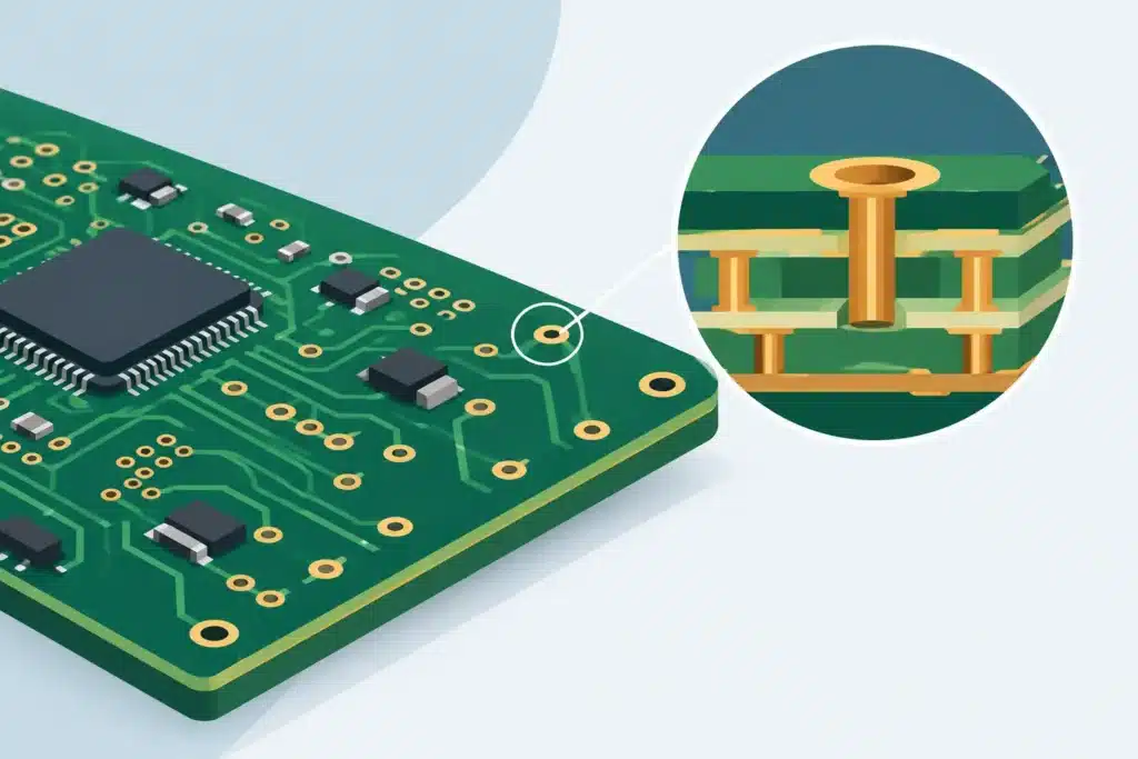
In a microstrip configuration, the trace resides on an outer layer with an underlying reference plane. In a stripline configuration, the trace is embedded between two reference planes. Both topologies are standard in professional designs, yet their electrical behaviors diverge significantly. Microstrip provides direct accessibility and is often advantageous for RF routing, whereas stripline typically delivers superior shielding and lower radiation in dense high-speed designs. The choice depends on frequency range, EMI risk profiles, layer counts, BGA breakout constraints, and manufacturing economics.
The governing parameters include trace width, post-etch copper thickness, dielectric thickness to the reference plane, dielectric constant (Dk), and the impact of the solder mask. For differential pairs, the edge-to-edge trace spacing is an additional factor; altering this spacing shifts the mutual coupling and, consequently, the differential impedance.
Furthermore, traces must not be evaluated in isolation. A 100-ohm pair is only effective if both conductors are routed symmetrically, refer to the same plane, and avoid unneeded asymmetries. Dissimilar via transitions, inconsistent clearances to copper flooding, or splits in the return path can convert differential-mode energy into common-mode noise, degrading both signal integrity and EMC compliance.
The return path is an integral part of the transmission line
High-speed signals do not simply propagate along the forward conductor. The return current seeks the path of least inductance, typically traveling directly beneath the signal trace on the adjacent reference plane. If that reference plane is disrupted by a plane split, cutout, or poorly positioned via field, the return current is forced into an expanded loop.
The direct results are increased loop inductance, impedance discontinuities, and elevated radiated emissions. A continuous reference plane is therefore not an aesthetic layout preference—it is a strict electrical prerequisite. During layer transitions, the return path must be actively managed, often by placing ground stitching vias immediately adjacent to the signal vias when crossing reference planes.
Stackup must be finalized prior to critical routing
A production-ready stackup explicitly specifies layer configuration, copper weights, prepreg thicknesses, core dimensions, and laminate material grades. It forms the foundation for impedance modeling, HDI architectures, via structures, thermal dissipation, and manufacturability. When critical nets are routed before the stackup is confirmed, teams inevitably face a tradeoff between compromised impedance and costly rerouting.
A common pitfall is utilizing a generic stackup derived from an earlier prototype or a standard CAD library. Even if the layer count matches, differences in the manufacturer's prepreg glass styles, copper foil profiles, and press-out cycles alter the final dielectric thickness. At higher frequencies, the laminate’s Dk and dissipation factor (Df) become increasingly critical to impedance tolerance and insertion loss.
The correct approach involves securing the fabricator's validated stackup early, assigning impedance constraints by net class, and resolving geometries against the actual buildup. For high-reliability designs, define how the fabricator is permitted to adjust trace widths to hit target values. This impedance compensation can be practical, but it must be governed and documented rather than handled as an unmonitored factory adjustment.
Vias, pads, and component transitions can compromise performance
Achieving nominal impedance across uniform traces does not inherently guarantee high-speed channel performance. Discontinuities introduced at BGA breakouts, connectors, test points, vias, and AC coupling capacitors can generate signal reflections. While moderate edge rates may tolerate substantial mismatches, high-speed serial links quickly deplete their timing and noise margins.
A through-hole via leaves behind an unused stub that behaves as a resonant open-circuit stub. Techniques such as backdrilling, blind vias, or optimized layer assignments mitigate this issue, though they introduce processing complexity and fabrication cost. These measures are not universally required; the decision must be driven by edge rates, channel loss budgets, via barrel lengths, and allowable reflection thresholds—rather than a blanket rule to backdrill every via.
Via padstacks and antipads require equal scrutiny. Insufficient or oversized antipads alter local parasitic capacitance. In dense HDI layouts, these discontinuities can prove more detrimental than trace variations. In these cases, 3D electromagnetic field solvers are indispensable, particularly for RF transitions, high-speed SerDes lanes, and critical connector launch designs.
Specifying requirements for the PCB fabricator
A rigorous fabrication drawing avoids vague notations like “controlled impedance.” Instead, it explicitly defines the trace geometry and target values—for example, a 50-ohm single-ended trace on outer layers referenced to L2, or a 100-ohm differential pair on an internal signal layer sandwiched between two ground planes.
The drawing must map each impedance class to its respective layers, specify allowable tolerances, and define verification criteria. If impedance is critical to system operation or compliance, the fabrication documentation must unambiguously state requirements for test coupons, measurement methodology (TDR), and acceptance criteria. Without these details, two production lots adhering strictly to the same Gerber files can exhibit divergent electrical performance.
Simultaneously, requirements must balance design margins with manufacturing reality. Tighter tolerances necessitate stricter process windows, specialized testing, and higher fabrication costs. A ±10% tolerance is typically sufficient for designs with robust margins. For high-precision RF filters or sensitive wideband links, specifying ±5% and selecting high-grade RF laminates may be warranted. Imposing unverified tolerances without electrical justification increases manufacturing risk, lead time, and cost without adding real engineering value.
Controlled impedance is a subset of signal integrity
Impedance matching cannot be resolved independently of the broader PCB design ecosystem. Line terminations, driver output impedance, receiver characteristics, Power Distribution Network (PDN) noise, interconnects, cable assemblies, and layout return paths all dictate composite signal integrity. A pristine 50-ohm trace is rendered ineffective if rail collapse shifts receiver thresholds or if a connector launch introduces a severe impedance discontinuity.
This applies equally to EMC. Precise impedance control and unbroken reference planes measurably reduce radiated emissions, yet they do not replace methodical floorplanning, filtering, decoupling, and chassis grounding. Electrical requirements must be synthesized into a cohesive layout that is fully manufacturable and stable throughout the product's operating lifecycle.
At Wise Choice Support, controlled impedance is executed as a rigorous engineering parameter: spanning stackup synthesis, field-solver modeling, layout routing, return-path verification, and fabricator alignment. This methodology mitigates the risk of critical signal integrity failures surfacing when hardware reaches the test bench.
The most critical time to address controlled impedance is prior to routing the first high-speed net. Finalizing the stackup, net topologies, and reference planes early ensures a predictable design cycle and delivers a finished circuit board engineered to perform strictly to specification.