A 10 Gbit/s link rarely fails because the physical routing is missing. It fails because the return current is forced into a detour, because the impedance shifts across a via transition, or because the power distribution network cannot deliver clean power at the circuit's actual operating frequency. High-speed PCB design is therefore not about routing traces quickly. It is about precisely managing electromagnetic energy throughout the entire printed circuit board.
For engineering teams in telecommunications, radar, medical technology, data center equipment, and defense, the consequence is tangible: A layout that appears correct in the CAD tool can still result in bit errors, emissions issues, near-zero timing margins, or unacceptable manufacturing variations. These issues are resolved far more cost-effectively during the design phase than after the first prototype or, worse, after the product has been released.
High-speed PCB design begins with the requirements
The concept of high-speed is not defined by clock frequency alone. The decisive factors are signal edge rate, transmission line length, and allowable margins. A digital signal with fast edge rates can demand the same rigor as a significantly higher clock frequency, because the high-frequency harmonics dictate the signal's behavior on the board.
Before layout begins, the electrical requirements must be translated into concrete design rules. This includes interface standards, data rates, differential impedance, single-ended impedance, maximum insertion loss, acceptable reflections, jitter budgets, and timing constraints. For RF and mixed-signal designs, isolation, coupling, phase control, and reference plane requirements must also be addressed.
This is also where decisions regarding PCB fabrication technology must be made. Layer count, material selection, copper weights, dielectric thicknesses, HDI architecture, and permissible via types are not manufacturing details that can be postponed. They are integral to the electrical design. A stackup that does not support the required impedances and return paths cannot be salvaged by subsequent routing discipline.
The stackup is the electrical foundation
A well-designed stackup places signal layers in close proximity to continuous reference planes. This provides controlled impedance, low return path inductance, and superior inter-layer shielding. The dielectric height between the signal and the reference plane directly dictates trace width, impedance, and field distribution. Consequently, the stackup must be coordinated with the specific PCB fabricator and validated against their process capabilities.
There is no single universally correct stackup. A compact HDI board with fine-pitch BGAs imposes different constraints than a large, high-power board or an RF design featuring sensitive analog sections. However, the principle remains constant: The layer stackup must be electrically justified, manufacturing-realistic, and fully documented before critical traces are routed.
Signal integrity depends on the entire interconnect path
When interconnect length becomes electrically significant, a copper trace behaves as a transmission line. Impedance discontinuities at connectors, vias, pads, stubs, and reference plane transitions induce reflections. On an eye diagram, this manifests as reduced eye opening, increased jitter, and degraded margins. In practice, this can lead to intermittent faults that are difficult to reproduce, as they depend on temperature, load, and component-to-component variations.
Controlled impedance does not merely mean that a trace has a calculated width. The impedance must be preserved across the entire interconnect. This requires precise management of trace width transitions, copper geometry, dielectric spacing to reference planes, via transitions, and component breakout launches. Differential pairs must remain tightly coupled, yet not so close that mutual coupling alters the targeted differential impedance. Furthermore, they must maintain uniform geometry with minimal asymmetries.
Length matching is a classic example of why design rules must be applied with technical insight. For DDR interfaces, parallel buses, and certain serial links, inter-signal timing is critical. However, unnecessary meanders can introduce losses, coupling, and unwanted resonances. The objective is not necessarily identical physical lengths, but correct electrical delay within the interface specification.
Return current must never be an afterthought
High-frequency current does not follow the path of least geometrical resistance. It follows the path of least impedance, typically directly beneath the signal trace on the reference plane. If a signal crosses a plane split or transitions from one reference layer to another without a controlled return path, a current loop is formed. This increases noise, electromagnetic radiation, and the risk of signal degradation.
During layer transitions, the signal via and return path must be treated as a single structure. Stitching vias placed in close proximity to the signal transition provide a low-inductance path for the return current between the relevant reference planes. This is especially critical for differential pairs, high-speed clocks, RF interconnects, and signals traversing layers with disparate reference planes. A layout may exhibit correct impedance on straight trace segments and still fail at every transition.
The PDN must supply power at dynamic load frequencies
Power integrity is inextricably linked to signal integrity. When an FPGA, processor, or high-speed ADC switches state, transient currents stress the power distribution network across a broad frequency spectrum. Excessive PDN impedance induces rail collapse and voltage ripple. This can shift threshold levels, increase jitter, and induce system faults that are frequently misdiagnosed as software anomalies or signal integrity issues.
An effective PDN relies on optimized plane geometry, localized decoupling, low-inductance interconnects, and a deliberate distribution of capacitor values. Simply increasing the number of capacitors is not a solution in itself. Placement, pad geometry, via loop inductance, and the circuit's transient current profile are far more critical than component count alone. The capacitor must be electrically close to the dynamic load it supports.
Plane pairs provide inter-plane capacitance, while closely coupled power-ground pairs minimize loop inductance. Concurrently, anti-resonances between discrete decoupling capacitors and plane structures must be mitigated. In this context, simulation is invaluable, as it identifies problematic impedance peaks prior to layout freeze. Adjusting the stackup and decoupling strategy in simulation is significantly more cost-effective than troubleshooting power instability on physical hardware.
EMC is a layout discipline, not a post-design test
EMC issues frequently originate at the interface between circuit functionality and physical layout implementation. High-speed current loops, discontinuous return paths, common-mode cable radiation, and inadequate board partitioning can prevent an otherwise functional product from achieving compliance. A late-stage EMC test merely indicates a compliance failure; it rarely identifies which specific layout decision caused the issue.
Therefore, EMC must be engineered into component placement and layout partitioning from the outset. Noisy switch-mode power supplies should be physically isolated from sensitive analog circuitry. High-speed lines routed to I/O connectors require unbroken reference planes along their entire length, and interface filters must be placed to prevent layout-level cross-coupling between filtered and unfiltered domains.
A continuous ground plane serves as the most effective reference. Splitting ground planes is often adopted as an intuitive solution for isolating analog and digital noise; however, it introduces severe integrity issues if high-speed signals are forced to cross the plane boundaries. In most designs, disciplined component placement, controlled current return paths, and proper signal referencing are far more effective than aggressive split planes.
Via topology and manufacturability must align
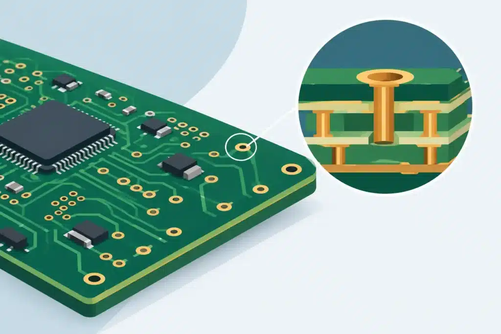
Vias are indispensable, yet they are not electrically transparent. A standard through-hole via leaves an unused via stub that behaves as an open-circuit resonant stub at high frequencies. Backdrilling, blind vias, or microvias may be required to eliminate stub resonance and facilitate dense breakout routing beneath fine-pitch BGAs. Conversely, these techniques increase fabrication complexity, cost, and process control requirements for the manufacturer.
Selecting the appropriate via architecture depends on interface performance requirements, routing density, production volume, and operational environments. Specifying advanced HDI provides no advantage if a standard through-hole build with an optimized stackup satisfies the signal loss budget. Conversely, selecting a lower-cost via structure is a false economy if it introduces signal degradation or forces design compromises on critical nets.
Production readiness also demands rigorous design rules governing annular rings, solder mask clearances, copper balance, thermal relief connections, panelization, and testpoint access. Design for Manufacturability (DFM) must never conflict with signal integrity. Both disciplines must converge in every layout decision, particularly under IPC Class 2 and Class 3 standards, where error margins are minimal and documentation requirements are stringent.
Pre-prototype verification prevents costly design iterations
Mission-critical designs require systematic technical reviews prior to the release of Gerber and fabrication data. Automated DRC checks within CAD tools are necessary, but they do not detect complex electromagnetic phenomena. A comprehensive design review must inspect return current continuity, reference plane transitions, via stubs, decoupling effectiveness, crosstalk coupling risks, thermal management, and manufacturing tolerances.
Signal integrity, power integrity, and targeted EMC simulations yield the greatest value when applied methodically. Simulating every trace is rarely necessary, but critical links, high-speed clocks, power distribution networks, and RF launches must be prioritized, as failures in these areas jeopardize system-level performance. Empirical measurements on the initial prototype should validate pre-layout assumptions, rather than serve as the first electrical evaluation of the design.
Wise Choice Support applies this rigorous discipline from architectural definition to production-ready layout: requirements, stackup design, routing, simulation, and design reviews are executed as a single, cohesive engineering process. This ensures streamlined decision-making and clear accountability for the technical details that determine whether a printed circuit board performs reliably without costly surprises.
When a high-speed PCB must operate reliably in mission-critical environments, success rarely hinges on a single major decision. It is the cumulative result of strictly controlled technical details—and the commitment to address them rigorously before they manifest as functional failures.