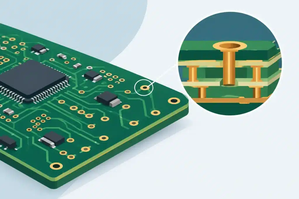
A PCB layout can appear finished long before it is technically complete. The components fit on the board, the netlist is fully connected, and the routing is done. However, if return currents, stackup, PDN, impedances, thermal behavior, and manufacturing tolerances are not addressed as a unified discipline, issues often surface only during bring-up, EMC testing, or production. An external PCB designer is therefore not merely an extra pair of hands for routing. It represents senior-level expertise for the decisions that determine whether the hardware operates reliably on the first revision.
For companies developing telecommunications, radar, medical devices, industrial electronics, defense, or data center equipment, PCB layout flaws are rarely minor. An unexpected resonance, a noisy power rail, or insufficient isolation between RF domains can substantially delay a project. When faced with compressed development schedules and limited internal specialist capacity, the external resource must be able to step directly into the design and take full ownership of the technical details.
When Does an External PCB Designer Make Sense?
The optimal time is not necessarily when the internal engineering department lacks layout bandwidth. Frequently, the need arises when the technical risk of the project exceeds the internal team's current domain experience. This applies, for example, to a first high-speed design featuring DDR, SERDES, or PCIe; a compact HDI board with fine-pitch BGAs; or a platform where EMC compliance governs the entire mechanical and electrical architecture.
An external specialist is also valuable when bringing an existing design back on track. The challenge might stem from failed EMC tests, unstable signal integrity, hot components, or low manufacturing yield. In such cases, simply moving a few traces or adding ferrite beads without a rigorous root-cause analysis is insufficient. The layout must be evaluated comprehensively, encompassing stackup, component placement, power distribution, reference planes, and fabrication constraints.
There is a fundamental difference between procuring layout drafting capacity and engaging advanced PCB specialist expertise. For straightforward controller boards, a standardized routing process may suffice. For high data rates, sensitive analog signals, RF, high power, or stringent operational reliability requirements, hands-on experience with specific physical failure mechanisms becomes essential.
Technical Responsibility Begins Before Routing
A production-ready printed circuit board does not begin with the first routed trace. The critical stage is establishing a design baseline where electrical, mechanical, and fabrication requirements are fully aligned. Resolving these factors during routing invariably leads to design compromises, unnecessary layer counts, or late-stage mechanical modifications.
Stackup and Controlled Impedance
A stackup is an electrical architecture, not merely a layer arrangement. The selection of dielectric materials, copper weights, plane spacing, and signal layer allocation dictates whether differential pairs and single-ended interfaces stay within specified impedance tolerances. It also directly governs the return current paths, fundamentally impacting both signal integrity and EMC performance.
An experienced PCB designer collaborates directly with the target fabricator to define the stackup, deriving trace geometries from actual manufacturing capabilities and material parameters. Assumptions based on standard impedance charts or generic rules from legacy boards are insufficient when tolerances, materials, and layer counts vary.
PDN, Decoupling, and Return Currents
Power integrity is frequently addressed too late in the development cycle. A schematic may contain all necessary decoupling capacitors in the bill of materials, yet the board can still suffer from an inadequate PDN. Component placement, via loop inductance, plane geometries, current paths, and the dynamic characteristics of voltage regulators dictate whether the distribution network can deliver current transients without intolerable voltage fluctuations.
This is particularly critical adjacent to FPGAs, processors, high-speed transceivers, and RF circuits, where layout decisions directly dictate jitter, bit errors, emissions, and functional stability. An external specialist must identify critical current loops and determine which power domains necessitate detailed simulation or strict design constraints.
Component Placement and Return Paths
Effective placement alleviates routing congestion, but its primary value is electrical. Interfaces must follow strict signal flow, noisy and sensitive circuits must remain isolated, and connections to connectors, antennas, sensors, or power stages require clearly defined, low-impedance return paths. A signal trace never exists in isolation: every high-speed transition generates a return current that seeks the path of least impedance on the adjacent reference plane.
When a trace crosses a plane split, transitions layers without nearby stitching, or traverses perforated reference planes, large loop areas are inevitably created. This results in signal reflections, common-mode noise, and radiated emissions. Rectifying such flaws after the first prototype revision is significantly more complex and costly.
From Schematic to a Manufacturable Assembly
A PCB can be electrically sound while remaining difficult or cost-prohibitive to manufacture. Consequently, design for manufacturing must be integrated continuously throughout the layout phase, rather than treated as a checklist verification prior to Gerber or ODB++ generation. The selection of microvias, blind/buried vias, annular ring sizes, trace clearances, pad geometries, and copper balance directly affects unit cost, fabrication yield, and delivery reliability.
HDI is a prime example. The technology may be essential for escape routing fine-pitch BGAs or reducing overall board size, but it introduces strict requirements for via architectures, sequential lamination cycles, and fabricator process windows. The optimal solution is rarely to maximize HDI layers arbitrarily; rather, it is to meet density and performance targets through a verified, repeatable manufacturing process.
The same principle applies to IPC Class 2 and Class 3 standards. Specifying a class is critical, but it does not replace precise fabrication notes. Critical nets, thermal soldering profiles, via fill specifications, test point access, creepage, and clearance must reflect the exact operating environment. For mission-critical electronics, documentation must clearly communicate acceptable criteria to the fabricator, assembly house, and test engineers alike.
Maximizing Value from External PCB Expertise
Collaboration is most effective when the external PCB designer is engaged early enough to influence hardware architecture and design constraints. If the specialist is only brought in after the schematic is finalized and mechanical dimensions are frozen, fundamental architectural decisions are already locked. While a proficient layout can still be delivered, design flexibility is restricted, and the risk of sub-optimal compromises increases.
An efficient engagement typically relies on a well-defined set of design inputs: updated schematics and netlists, mechanical outlines and keep-outs, component specifications, known constraints, production volume targets, test strategy, and EMC or environmental specifications. For high-speed interfaces, requirements regarding data rates, topologies, length matching, impedances, and vendor design guidelines must be clearly established. Clarifying ambiguities upfront is vastly superior to masking uncertainty during routing.
Communication channels are equally critical. On complex hardware projects, direct technical dialogue between the lead hardware engineer and the layout specialist minimizes misinterpretations compared to communicating through administrative layers. At Wise Choice Support, clients work directly with Principal PCB Design Specialist Steen Kaare Grøndahl. This provides direct decision-making and clear accountability: technical trade-offs, risks, and necessary compromises remain transparent while they can still be actively resolved.
Design Reviews Beyond Final Gate Checks
A design review delivers maximum value when utilized as a formal engineering gate throughout the layout process. Prior to component placement, the review validates preliminary placement, mechanical keep-outs, and stackup feasibility. Prior to tape-out, it verifies routing topologies, reference plane continuity, impedance targets, PDN robustness, EMC mitigation, thermal distribution, and DFM compliance.
When assessing an existing design, a review should start with the observed symptom but delve deeper into root causes. If a board fails an emissions compliance test, the analysis must go beyond identifying the offending frequency peak. It must pinpoint the underlying coupling mechanism and the layout geometry that enables it. Otherwise, the engineering team risks implementing expensive, trial-and-error revisions that yield marginal results.
Simulation provides valuable verification, especially for critical signal channels, PDN impedances, and RF structures. However, simulations are only as accurate as their models, boundary conditions, and physical assumptions. They are an engineering aid, not a substitute for hands-on layout expertise, empirical validation, and rigorous evaluation of real-world operating environments.
Evaluate by Risk Profile, Not Merely Hourly Rates
When procuring external engineering support, companies frequently weigh hourly rates before evaluating technical depth and engineering accountability. While understandable, this approach is inherently flawed for mission-critical hardware. A lower hourly rate quickly becomes expensive if a design requires protracted review cycles, an extra prototype spin, or extensive redesign following EMC compliance failures.
Instead, assess whether the PCB designer possesses proven expertise aligned with the project's specific risk profile: specific high-speed protocols, RF systems, complex HDI, stringent EMC standards, IPC Class 3 compliance, or process yield challenges with designated fabricators. Demand clear parameters regarding deliverables, applied design rule sets, and layout sign-off protocols. Additionally, define ownership of fabricator communication and processes for managing changes driven by component obsolescence or mechanical updates.
An external PCB designer should never artificially simplify a complex hardware project. The core mandate is to make technical complexity manageable, document critical design decisions, and translate system specifications into a robust, manufacturable printed circuit board engineered to perform reliably under its designated operating conditions. This discipline allows your internal development team to focus on core product innovation rather than resolving downstream layout defects.