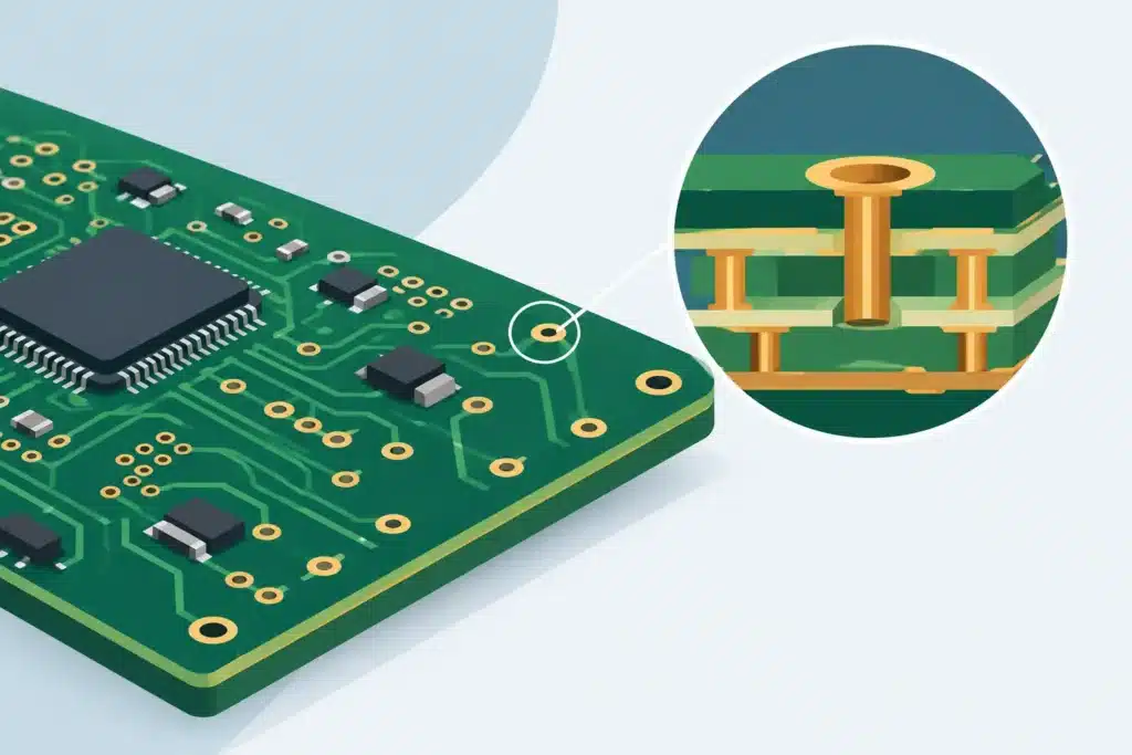
An EMC test that fails late in the development cycle is rarely a single component issue. More often, it is the cumulative result of minor layout decisions that have collectively created unintended current loops, resonances, or common-mode noise. PCB EMC optimization must therefore begin while the architecture, stackup, and component placement can still be influenced—not when the product is already in the test lab.
For complex products within sectors such as medical devices, telecommunications, radar, defense, and industrial electronics, EMC is not an isolated discipline. It is directly tied to signal integrity, power integrity, mechanics, cabling, enclosure design, and manufacturing choices. A printed circuit board may function electrically on the lab bench and still fail once installed in its final chassis, connected to cables, or subjected to fast transients.
PCB EMC Optimization Begins with the Current Path
EMC fundamentally revolves around the coupling between a noise source, a coupling path, and a receptor or antenna. A fast digital edge is not inherently problematic on its own. The problem arises when the return current cannot closely track the forward current, or when energy gains access to structures capable of radiating.
On a PCB, high-frequency return currents follow the path of least inductance—typically directly beneath the signal trace in the adjacent reference plane. If a signal crosses a split in the GND plane, traverses between layers without adequate stitching, or transitions references without an adjacent return path, the current is forced into a larger loop. This increases both emissions and susceptibility to coupled noise.
Therefore, EMC must be evaluated at every critical routing decision. This applies especially to clocks, differential pairs, high-speed interfaces, switch-mode power supplies, and signals leaving the board via connectors or cables. A layout with short traces is not automatically compliant from an EMC perspective. The decisive parameter is the entire current path, including the return path.
The Stackup is an Electrical Construction
Stackup is often selected based on layer count, cost, and routing density. While these are necessary considerations, they are insufficient in an EMC-critical design. The layer stack defines impedance, coupling between signal and reference planes, power plane capacitance, and the ability to control return currents.
A signal layer with an adjacent, continuous reference plane provides a predictable transmission line. This reduces loop inductance and confines field propagation. The dielectric separation between the signal and reference planes has a direct impact: tighter coupling improves field containment, but simultaneously demands precise impedance calculations and realistic manufacturing tolerances.
In designs featuring high-speed interfaces, the stackup should therefore be defined in coordination with the PCB fabricator's material data. Dielectric constant, copper thickness, prepreg flow, and etching all affect the final impedance. A controlled impedance callout on the drawing holds little value if it fails to align with the actual layer buildup and the chosen fabrication process.
Planes Must Serve a Defined Purpose
As a rule of thumb, a GND plane should remain continuous. Cutouts, narrow bottlenecks, and splits may be necessary for safety or isolation requirements, but they must be treated as active EMC elements. If a signal must cross such a structure, the return current must be provided with a defined alternative path.
Power planes can support the PDN, but they do not replace a solid GND reference plane. Particularly in mixed-signal designs, failures often occur when analog and digital domains are split mechanically without analyzing current paths. The objective is not to isolate everything. The objective is to control where noise currents flow and prevent them from traversing sensitive circuitry.
The PDN Often Dictates the EMC Margin
Many radiated and conducted emission issues originate within the power distribution network. A switching regulator with fast current transitions, insufficient decoupling, or a physically large hot loop can generate broadband noise that couples across the entire board. That same PDN can also leave a product susceptible to EFT, burst, or other transient disturbances.
Decoupling capacitors operate effectively only when the interconnect to the IC’s power and GND pins exhibits very low inductance. This demands short, wide traces and vias placed so that the current avoids detour loops. A capacitor placed close to the component, but connected via long, thin traces, can prove largely ineffective at high frequencies.
Power integrity and EMC must therefore be addressed cohesively. The PDN impedance must remain low and controlled throughout the frequency range where load steps generate current variations. This involves not only capacitor values, but also their ESL, placement, plane pairs, via inductance, and the regulator layout. Adding more capacitors is not always the correct remedy. Improperly selected values can introduce anti-resonances, exacerbating noise within critical frequency bands.
Component Placement Mitigates Issues Prior to Routing
The most meticulous routing cannot fully compensate for flawed component placement. Noisy circuits such as DC/DC converters, clock generators, and high-speed digital interfaces must be located with strict consideration for sensitive analog circuitry, RF front-ends, sensors, and connectors.
Connectors demand particular attention because attached cables readily act as efficient antennas. Common-mode current on a cable is a primary driver of emissions compliance failures. Filtering, ESD protection, and potential common-mode chokes must be positioned directly at the interface so that unwanted energy is suppressed before penetrating the rest of the board. A protection component placed several centimeters away from the connector leaves a trace stub that can still radiate noise or pick up transients.
Enclosure bonding and chassis GND must also be resolved early in the design phase. There is no single universal solution for every product. The appropriate coupling strategy between signal GND and chassis depends on frequency ranges, cable types, isolation, regulatory safety requirements, and mechanical architecture. The critical factor is that the choice is deliberate and executed consistently throughout the layout.
Vias and Layer Transitions Can Compromise an Otherwise Sound Layout
A signal via is not merely a convenient conductive connection between two layers. At high frequencies, a via introduces parasitic inductance, stubs, and a potential discontinuity in the return path. When a signal transitions between reference layers, the return current must transition alongside it. This is typically resolved using GND stitching vias positioned immediately adjacent to the signal via, or via appropriate capacitive coupling between reference planes, depending on the stackup design.
The same principle applies to differential pairs. The pair must maintain its geometry, but it also requires a continuous reference and symmetrical transitions. Unnecessary vias, asymmetrical reference conditions, and poorly positioned plane cutouts can convert differential-mode energy into common-mode noise. It is precisely this common-mode noise that cables, connectors, and enclosure apertures readily radiate.
For multi-gigabit interfaces, backdrilling, via geometry optimization, and connector launches may become essential focal points during design reviews. Here, EMC, signal integrity, and manufacturing economics are deeply intertwined. An advanced via structure may be technically optimal, but it must be balanced against via counts, fabrication complexity, and the actual margins of the system.
EMC Cannot Be Validated by Design Rules Alone
Layout guidelines and checklists are valuable tools, but they do not replace technical engineering judgment. Two designs can adhere to identical rule sets and exhibit radically different behavior due to component parasitics, cable harness environments, enclosure geometry, and operating states.
A rigorous design review must therefore track energy propagation throughout the product: Where do high-frequency currents originate? Which signals contain the highest harmonic content? Where can return currents be disrupted? Which structures could serve as antennas? And where can external noise couple into the system?
Measurement should be employed to validate or disprove specific engineering hypotheses. Near-field probes, RF current probes, and pre-compliance measurements can pinpoint dominant noise sources early. Conversely, test data evaluated without reference to layout and system architecture often leads to arbitrary modifications—such as adding ferrite beads, additional capacitors, or rerouting traces without identifying the root cause.
Production-Ready EMC Requires Documented Engineering Decisions
An EMC-compliant prototype board is not automatically a production-ready board. Substrate material substitutions, copper balance adjustments, solder paste variations, component alternatives, and cable assembly discrepancies can shift EMC performance. For critical products, the stackup, impedance specifications, PCB fabrication notes, component placement, and test points must be rigorously documented to ensure manufacturing repeatability.
Wise Choice Support addresses EMC as an integral part of comprehensive PCB design—from stackup and PDN to routing, HDI structures, and manufacturing documentation. This expertise is particularly vital when troubleshooting an existing design or when building EMC margins into the hardware prior to the first prototype spin.
The most impactful EMC optimization is often the one executed before a single trace is routed: an optimized stackup, a relocated connector, an unbroken reference plane, or a well-defined return path. This approach delivers robust margins, minimizes redesign cycles, and yields a printed circuit board that can be manufactured to faithfully preserve its intended electrical performance.