A regulator that loses efficiency at high junction temperatures, or an FPGA with uneven thermal dissipation, cannot be resolved with a few extra thermal vias at the end of the layout phase. The query “how to perform thermal analysis PCB” fundamentally covers a discipline where power dissipation data, stackup, component placement, copper geometry, and mechanical enclosures must be evaluated holistically. Flawed inputs produce appealing simulations, but poor design decisions.
Thermal analysis must therefore begin while the architecture and component placement can still be adjusted. The objective is not merely to keep individual components below their absolute maximum ratings. The goal is to document sufficient margin under realistic operating conditions, ensuring that service life, parametric performance, solder joints, and overall system reliability are not compromised.
How to Perform PCB Thermal Analysis
An effective analysis tracks thermal energy from the heat source to the surrounding environment. Power dissipation originates within the component, is conducted through the packaging and solder joints to the PCB, spreads through the copper layers and vias, transfers to the enclosure, heatsink, or ambient air, and finally disperses into the external environment. Each interface introduces thermal resistance. The weakest link invariably governs the result.
The process begins with an accurate definition of the analysis case. A PCB analysis for a telecommunications card in a forced-air rack involves fundamentally different boundary conditions than a sealed medical device or a space-grade unit operating with minimal convection. Ambient temperature, mounting orientation, airflow profile, chassis material, adjacent assemblies, and duty cycles cannot be treated as afterthoughts.
For each critical heat source, determine the dissipated power. Ideally, this is measured on representative hardware or calculated based on datasheets, supply rails, operational load profiles, and expected efficiency. Distinguishing between typical and worst-case power dissipation is essential. A DC/DC converter, processor, or RF power amplifier may experience transient peak loads, whereas specific fault conditions lead to prolonged thermal stress. Both scenarios can be dimensioning factors, but they impose distinct requirements on the analysis.
Build a Model That Accurately Reflects the Physical Product
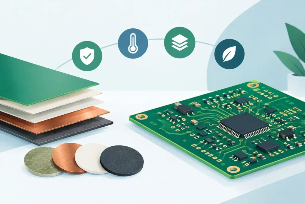
A thermal model is only as accurate as its geometry and material definitions. The PCB stackup must therefore mirror the intended fabrication baseline: layer count, copper weights, dielectric materials, prepreg, core, copper plane distribution, and finished copper thicknesses. In multilayer boards, internal copper planes generally exert a far greater influence on heat spreading than the dielectric substrate, but their efficacy depends on whether they are effectively thermally coupled to the heat sources.
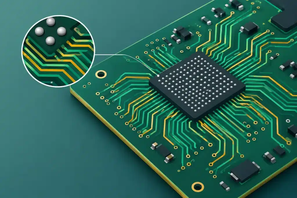
Component footprints must likewise be modeled realistically. A QFN with an exposed pad, a BGA with a high-density ball grid array, and a discrete power package with an integrated heat slug conduct heat along distinct paths. While manufacturer junction-to-ambient (theta-JA) metrics provide a preliminary estimate, these values are derived under standardized test setups and cannot be directly applied to a production design. Junction-to-board, junction-to-case, and transient thermal impedance data are significantly more reliable inputs.
For complex assemblies, the model is typically constructed within a 3D thermal simulation tool incorporating PCB geometry, critical components, enclosure mechanics, and active or passive cooling elements. Electrical power is assigned to the respective packages, with convective coefficients, contact resistances, and thermal boundaries defined accordingly. At elevated temperatures or within hermetically sealed enclosures, radiative heat transfer also becomes relevant, though it rarely offsets an inaccurate assessment of conduction and convective flow.
While it is tempting to model every geometric detail, doing so is often unnecessary. An early-stage analysis can utilize simplified component packages and focus exclusively on high-dissipation devices. The model can subsequently be refined as enclosure details, heatsink geometries, and airflow channels are finalized. Precision should be applied where it actively informs design decisions.
Define Boundary Conditions Before Interpreting Results
Inaccurate boundary conditions are the primary cause of misplaced confidence in thermal simulations. If a model assumes unobstructed airflow while the board is situated within a tightly packed multi-slot chassis, operating temperatures will be severely underestimated. Similarly, assuming ideal thermal contact with an aluminum enclosure without accounting for mechanical tolerances, surface finishes, or clamping pressure yields a thermal path that performs far better on screen than in the physical product.
Best practice dictates analyzing at least three operational states: nominal environment, specified maximum operating conditions, and a conservative worst-case scenario. For chassis-mounted assemblies, contact resistance across fasteners, thermal pads, and thermal interface materials (TIM) must be accounted for. In forced-convection systems, volumetric airflow and flow vectors must be realistic, factoring in pressure drops caused by air filters, wiring harnesses, and particulate buildup over time.
At the PCB level, evaluate whether adjacent components create cumulative heating. An isolated analysis of a single high-dissipation regulator may appear compliant, yet in the actual layout, that regulator may be placed adjacent to an FPGA, a power inductor, and an internal chassis wall. Operating temperatures are ultimately governed by the aggregate of all thermal paths and distributed heat sources.
From Hotspot Identification to Targeted Layout Optimization
When a simulation identifies a localized hotspot, adding vias is not a universal solution. The primary thermal path must first be identified. Is the bottleneck located at the junction-to-package interface, package-to-board transition, copper heat spreading, or dissipation from the board to the environment? Implementing a mitigation on the wrong side of the thermal bottleneck adds layout complexity and manufacturing cost without yielding meaningful thermal reduction.
When heat must be extracted from an exposed pad, a dense and properly dimensioned thermal via array should be routed to tie the top copper to internal and bottom ground planes. Via density, drill diameter, barrel plating thickness, and connection to copper planes all impact performance. Tented, filled, or capped vias may be required to maintain solder integrity during assembly, particularly under Bottom-Terminated Components (BTC) and BGAs. Concurrently, manufacturing capabilities and cost structures must be evaluated before freezing the design.
Increasing copper coverage lowers local thermal resistance, but this trade-off must be managed carefully. Plane expansions can compromise controlled impedance, return paths, creepage distances, and EMC performance. On high-speed digital and RF boards, thermal optimization cannot be executed without considering signal integrity and reference planes. An optimal layout achieves a balanced compromise between thermal performance, electrical integrity, and manufacturability—rather than simply maximizing copper surface area.
In select architectures, relocating components is the most effective corrective measure. Positioning a high-dissipation component near the board edge enables short thermal paths to a chassis or external heatsink, whereas locating it centrally can thermally stress surrounding subcircuits. In other scenarios, selecting a more efficient regulator topology, utilizing a larger package, modifying switching frequencies, or reducing electrical load represents the correct engineering response. The PCB can optimize thermal dissipation, but it cannot resolve fundamental circuit inefficiencies.
Validate the Simulation on Physical Hardware
Simulation mitigates design risk, but empirical testing on physical prototypes remains essential. Validation must be executed under representative load profiles, inside the intended enclosure, and across the specified ambient temperature envelope. Calibrated thermocouples provide highly accurate point measurements when bonded correctly. Thermal imaging offers a comprehensive overview of surface temperature distribution, though emissivity corrections, unpainted metallic surfaces, and reflections must be systematically managed for quantitative validation.
Correlate measured data directly with simulation results and account for discrepancies. Is the actual airflow lower than simulated? Is dynamic power consumption higher than projected? Is interface contact resistance higher than modeled? This correlation refines the thermal baseline for subsequent design iterations. For high-reliability and mission-critical products, thermal validation data also serves as the formal foundation for derating electrolytic capacitors, optocouplers, power semiconductors, and interconnects.
Establish Production-Ready Thermal Specifications
A thermal mitigation strategy must be repeatable in volume production. Consequently, explicit requirements for finished copper weight, via technology, via fill types, surface finish, thermal interface material (TIM) specifications, fastener torque limits, and assembly instructions must be detailed in the fabrication drawing and assembly documentation. A thermal design that depends on an operator manually aligning a thermal pad or applying a non-metered quantity of thermal paste is insufficiently controlled.
Thermal analysis is an integral element of a thorough design review prior to layout release. Wise Choice Support can evaluate whether power budgets, stackup architecture, component placement, and thermal transfer mechanisms align with relevant IPC standards and target manufacturing processes. This verification is critical for designs featuring HDI technology, heavy copper layers, high-density BGAs, RF power stages, and passively cooled systems.
The primary value of thermal analysis lies in providing concrete, actionable engineering guidance early enough to guide the layout architecture. Addressing thermal failures after hardware deployment invariably results in restricted design options, delayed production schedules, and significantly higher revision costs.