A differential pair can be routed with the correct impedance, proper spacing, and good length matching—and still fail the EMC test. The cause is often not the signal trace itself, but the path the return current is forced to take. Minimizing return-path disruptions is therefore a fundamental consideration in any high-speed, RF, or noise-sensitive PCB layout.
At high edge rates, the return current does not necessarily follow the electrically shortest path to the source. It concentrates beneath the signal trace on the nearest reference plane, where the field coupling—and thus the inductance—is lowest. If this reference is broken, the controlled return path is broken. The result can be an increased loop area, reflections, common-mode noise, crosstalk, and unpredictable EMC behavior.
Why a Disrupted Return Path Becomes a System Problem
A digital signal consists of more than just logical zeros and ones. The fast rising and falling edges contain energy far above the fundamental frequency. A 100 MHz clock with a short rise time can therefore place demands on the layout that are significantly higher than 100 MHz would suggest. It is the edge speed, the reference geometry, and the transitions between layers that determine how sensitive the design will be.
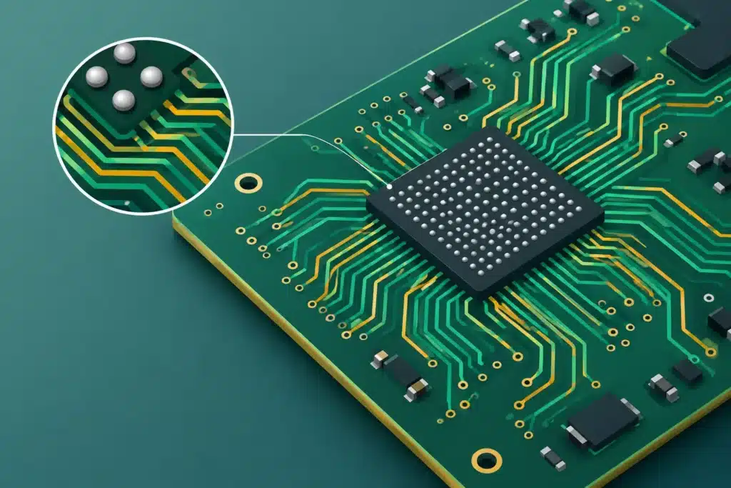
When a signal on an outer layer is connected to a continuous GND plane directly beneath the layer, high-frequency return current flows primarily beneath the trace. If the trace crosses a split, a milled-out area, a keepout zone, or the edge of a plane, the return current must take a detour. This detour increases loop inductance. During fast transients, even small inductances cause voltage fluctuations, which can manifest as jitter, overshoot, ringing, or radiated emissions.
The problem becomes particularly serious when multiple signals pass through the same discontinuity. Their return currents then share a limited path, creating a common-mode impedance. This can couple noise between otherwise independent interfaces and make errors dependent on system state, cable configuration, or load. It is precisely these errors that are often costly to reproduce and resolve late in the process.
How to Minimize Return Path Interruptions in Stackup and Routing
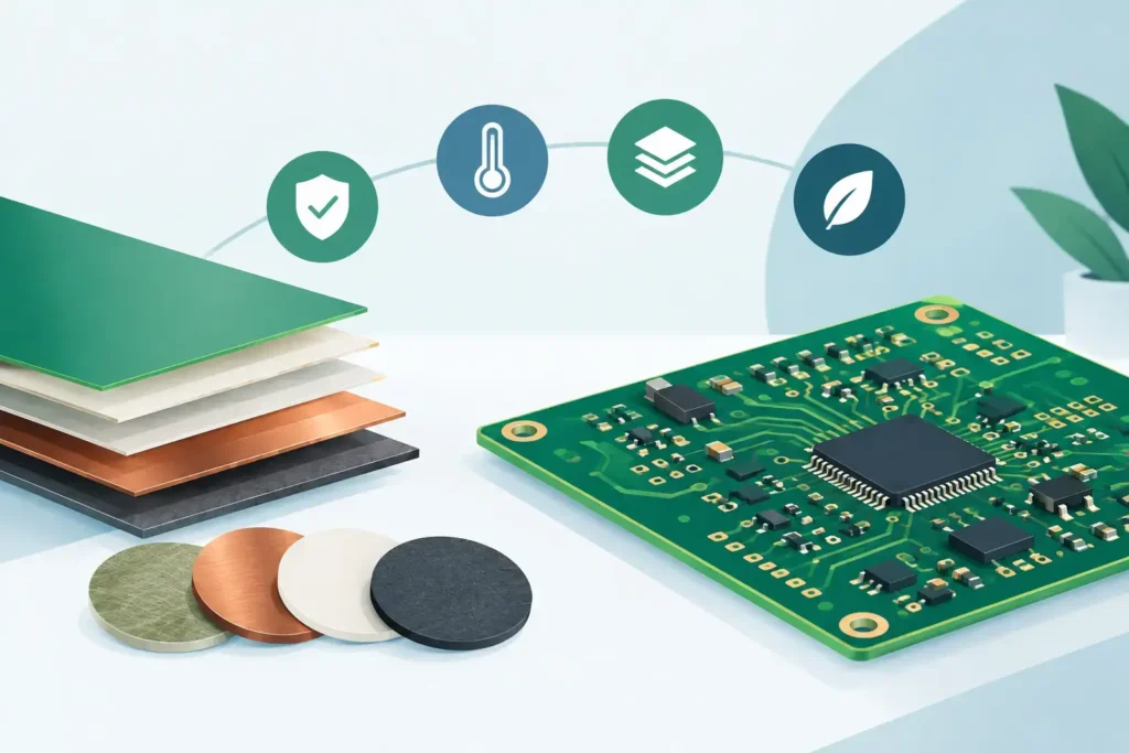
Prevention begins before the first trace is routed. The stackup must be defined with clear reference planes for each signal layer, controlled dielectric, and a deliberate strategy for power and ground layers. A signal layer without a dense, continuous reference plane is rarely a neutral choice. It is a compromise that must be technically justified.
For high-speed single-ended signals, a continuous GND reference is usually the most predictable solution. Ground serves as a common reference across interfaces and provides the return current with a clear, low-inductance path. Power planes can be used as a reference, but only when their impedance relative to GND is low across the relevant frequency range. This depends on the distance between the plane pairs, the decoupling strategy, capacitance, component placement, and frequency content. A power plane is not automatically an acceptable high-frequency reference simply because it is connected to GND via capacitors somewhere on the board.
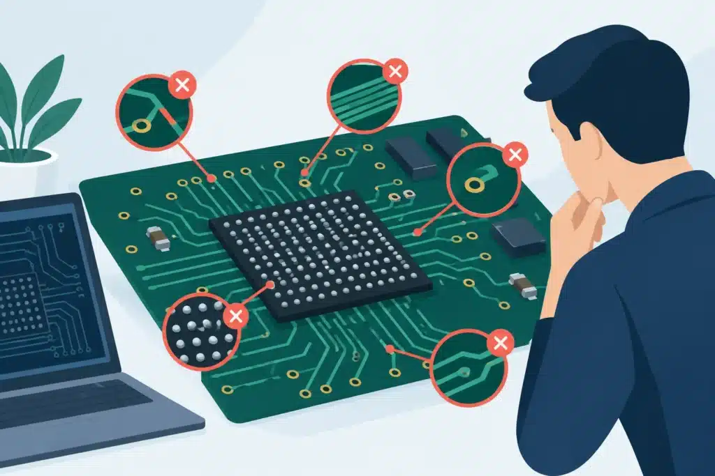
Avoid routing high-speed signals across plane splits, antipads, slots, and mechanical cutouts. This also applies to small breaks that may appear harmless in the layout view. A dense via fence, a series of plane clearances, or an elongated antipad area can create a real interruption for the return current that must follow a signal trace.
If a signal must pass through a local cutout, the layout should be modified before attempting to compensate with subsequent EMC measures. Move components, reverse the routing direction, adjust the plane geometry, or use a different signal layer with an intact reference. A layout that is physically neat but electromagnetically incorrect will not be improved by adding GND vias afterward.
A change in management requires a plan for the return flow
A via change does not merely alter the signal’s layer. It also often changes the plane to which the signal is referenced. If a signal travels from one layer with a GND reference to another layer with the same GND reference, the return current must be able to follow between the planes. Therefore, place one or more GND-stitching vias close to the signal via. The distance is critical: The farther the return current has to travel laterally to find a transition, the larger the loop becomes.
If the signal travels between layers that are referenced to different power planes, a dedicated AC return path between the two references is required. A properly placed decoupling capacitor can provide this coupling in some cases, but its placement, parasitic effects, and the relevant frequency range must be evaluated. A capacitor located several centimeters away does not provide a local return path for a fast edge transient.
The same principles apply to differential pairs. Ideally, the fields are primarily coupled between the two conductors, but the pair still has an external return current, especially when the geometry is asymmetrical, when the pair passes through vias, or when common-mode components arise. Differential routing therefore does not exempt the design from the requirement for continuous reference planes.
Keep GND continuous and the power supply local
A common mistake is to separate the GND for analog, digital, RF, or power and then allow the signals to cross those boundaries. The intention is to isolate noise, but the effect can be the opposite: the return current is forced away from the signal and forms large current loops. For most mixed-signal designs, a continuous ground plane with well-thought-out physical zoning is more effective than strict GND splits.
Instead, isolation must be achieved through placement, orientation, current paths, and decoupling. Noisy switch-mode areas, high-current loops, and sensitive analog front-ends are placed so that their fields and return currents do not overlap. This makes it possible to maintain a continuous GND reference while keeping critical functions electromagnetically isolated.
The power distribution network plays a similar role. If the current return from a load is forced through narrow connections, plane-to-plane gaps, or split areas, ground bounce and voltage modulation occur. This can degrade both signal integrity and converter performance, as well as increase emissions. Therefore, size the copper, via array, plane pairs, and decoupling based on the actual current transients—not just the DC current.
Evaluate the return path during a design review
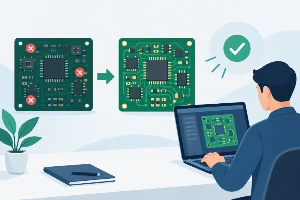
Return path errors are best detected systematically while the layout can still be modified without affecting the mechanical design, production, or schedule. During a design review, each critical interface should be traced throughout the entire connection: from the driver through the routing and vias to the receiver. For each segment, it must be determined which plane the signal refers to, where the return current flows, and how it adapts to layer or reference changes.
This includes, among other things, clocks, DDR, SerDes, Ethernet, USB, PCIe, ADC and DAC connections, switching nodes, and RF traces. However, even slower signals can be critical if they are located near sensitive analog circuits, connect to external cables, or share a reference with high-current circuits.
Also check the edges of planes beneath critical traces, GND vias near signal vias, connector pins, and transitions between the PCB and the cable. A cable often acts as an effective antenna if common-mode noise reaches the connector. A poor return path immediately before the connector can therefore cause an otherwise properly functioning board to fail in the overall product configuration.
Simulation can enhance critical assessments, especially at high data rates, with RF, and in dense HDI structures. However, simulation does not replace the discipline of physical layout. A properly defined stackup, consistent references, and short return paths are the fundamental conditions that make the analyses meaningful and ensure that production results are reproducible.
When Compromises Are Necessary
There are designs in which plane splits, mechanical slots, or areas with dense component placement cannot be avoided. In such cases, the compromise must be documented and addressed locally. This may involve rerouting, additional GND stitching, controlled reference transitions, a modified stackup, or the relocation of connectors and critical components.
There is no single universal spacing or via rule that works for every situation. It depends on rise time, frequency, trace spacing, impedance requirements, current profile, EMC targets, and the specific geometry. Therefore, the return path must be evaluated as part of the overall electromagnetic structure—not as an isolated rule check in the PCB design tool.
The most effective measures are taken early on: when the stackup, component placement, and plane structure can still be changed. An extra hour spent analyzing the return path before routing can save weeks of EMC troubleshooting, respins, and unreliable rework solutions. It’s this kind of detail that determines whether a complex printed circuit board can simply be manufactured or whether it will function reliably in the finished product.