An FPGA design may look entirely correct on the schematic and still fail in the lab when the core rail sags a few millivolts during a fast load transient. This is precisely the type of failure that a power integrity analysis must identify before the layout, stackup, and component placement are frozen. Average current rarely tells the whole story. Dynamic current, regulator control loops, capacitor parasitics, and PDN resonances dictate whether the power rail stays within specification.
For complex printed circuit boards, power integrity is not an isolated discipline to be added onto the layout at the final stage. It is inextricably linked to component selection, mechanical constraints, thermal management, signal integrity, EMC, and manufacturing capabilities. An analysis must therefore drive concrete design decisions—not merely generate a graph with an acceptable impedance curve.
What a Power Integrity Analysis Must Clarify
The objective is to verify that each critical supply rail delivers the required voltage at the point of load, even during fast current transients. The analysis encompasses the entire Power Distribution Network (PDN): VRMs or DC/DC converters, bulk capacitors, local decoupling capacitors, planes, vias, BGA breakout, component packages, and, in many cases, the on-die power grid of the IC itself.
The primary question is not how many capacitors to place. It is what voltage tolerance the device actually requires, and what current transient it must support. A processor with a 0.8 V rail and a tolerance of a few percent imposes entirely different PDN requirements than an analog 12 V supply for a gate driver. If the permissible voltage variation and the transient rise and fall times are undefined, dimensioning relies on assumptions.
From these parameters, a target PDN impedance can be established. The fundamental relationship is straightforward: allowable voltage ripple divided by maximum dynamic current yields the target impedance. In practice, the execution is more nuanced. The voltage budget must be allocated across DC drop, transient droop, regulator response, ripple, and noise coupling. Simultaneously, the IC's current profile shifts with operating modes, temperature, firmware execution, and load conditions.
Consequently, an impedance profile below the target threshold is a useful benchmark, but not an isolated sign-off criterion. A narrow impedance peak may be benign if it falls outside the spectral energy of the load transient. Conversely, it can be critical if excited by clock-related harmonics or the regulator's control loop. This requires evaluating the impedance profile in the context of the actual transient load.
From Current Profile to an Actionable PDN Model
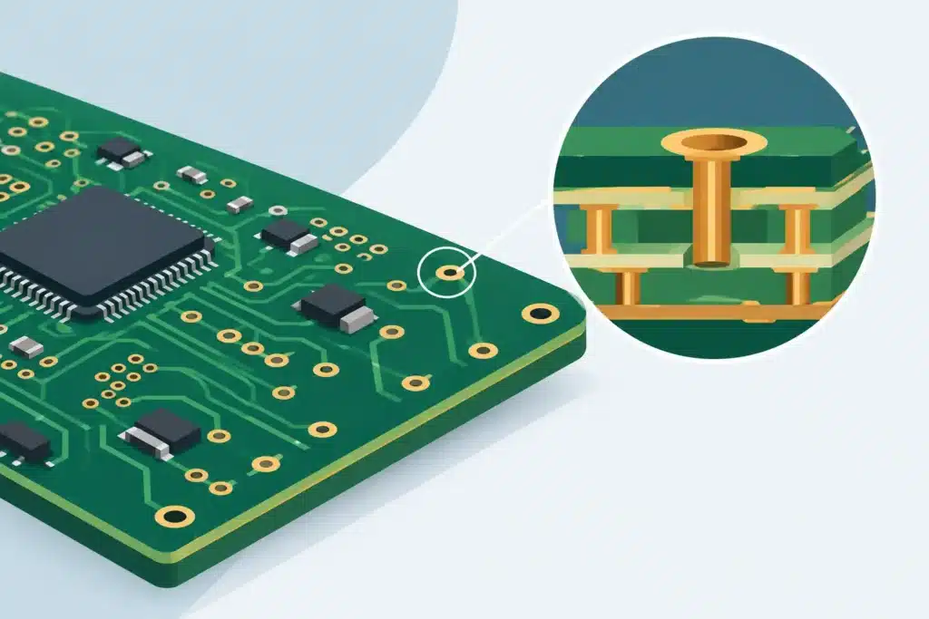
A reliable analysis begins with an accurate design baseline. This includes regulator performance data, DC-bias-dependent capacitance and ESR/ESL of capacitors, PCB stackup, copper weights, plane geometries, via arrays, and load locations. For BGA components, the breakout structure is often decisive. Extended trace lengths or insufficient power and ground vias can render an otherwise well-designed capacitor bank ineffective at high frequencies.
MLCC capacitors are a classic example of why nominal datasheet values must not be accepted at face value. A 10 µF capacitor can lose a significant portion of its effective capacitance under DC bias. Furthermore, package size, mounting inductance, and plane connections dictate the frequency at which the component actually contributes. Ten capacitors of identical nominal value are not inherently better than an engineered combination optimized for placement and low loop inductance.
The PDN model should be developed iteratively. First, the power distribution architecture and critical rails are defined. Next, DC resistance and copper IR drop are evaluated. Only when the stackup, footprint, via structures, and component placement are sufficiently mature does a broadband AC simulation of the physical PDN yield full value. This progression saves time by resolving fundamental architectural bottlenecks before descending into detailed layout implementation.
DC Analysis Extends Beyond Thermal Considerations
High current densities passing through narrow traces, plane neck-downs, and sparse via arrays cause both voltage drops and localized heating. At low supply voltages, a few millivolts are critical. This is especially true for FPGAs, ASICs, and high-performance processors, where the margin between normal operation and brownout can be razor-thin under peak utilization.
A DC IR drop analysis reveals whether current distributes as intended and identifies localized bottlenecks. It informs modifications to copper area, layer allocation, via stitching arrays, regulator placement, and remote sense line routing. These adjustments must be made while the layout remains flexible. Attempting to compensate for an inadequate current return path with additional decoupling capacitors is rarely viable.
AC Analysis Reveals Resonances and Local Noise
At higher frequencies, parasitic inductance dominates. Current cannot be supplied instantly from the voltage regulator or remote bulk capacitors; it must be delivered locally by decoupling capacitors and closely coupled plane pairs near the IC. The dielectric thickness between power and ground layers in the stackup governs plane capacitance and high-frequency noise propagation, while vias and mounting pads introduce the loop inductance that typically sets the operational limit.
Issues frequently arise in transition regions: where bulk capacitors lose effectiveness, where MLCCs reach their series resonance frequency (SRF), or where package and die parasitics begin to govern behavior. Anti-resonances between parallel capacitor branches can produce severe impedance spikes. Adding raw capacitance is therefore not inherently beneficial; performance depends on ESR, ESL, frequency coverage, and the overall damping of the PDN.
Layout Decisions with Maximum Impact
Translating analysis into PCB layout means prioritizing geometry over component count. Critical decoupling capacitors require short, wide, and low-inductance connections between power and ground. This typically necessitates placement on the bottom layer directly beneath the BGA, utilizing via pairs placed as close to the mounting pads as possible. A capacitor located a few centimeters away on the same rail is electrically distant at the frequencies where fast transient energy is demanded.
Continuous reference planes are equally critical. Split planes, copper voids, and unnecessary layer transitions disrupt return paths and elevate loop inductance. In HDI designs, microvias and via-in-pad technology can drastically reduce the current path, but the approach must be aligned with manufacturing capabilities, via fill requirements, reliability standards, and cost targets. The most compact geometry is counterproductive if it degrades fabrication yield or prevents reliable rework.
Regulator placement also demands rigorous engineering trade-offs. It must be situated close enough to the load to minimize DC losses, yet its switch node, magnetic fields, and high-di/dt loops must not compromise sensitive analog circuits, RF sections, or high-speed differential pairs. Power integrity and EMC are best addressed concurrently. A noisy regulator layout can simultaneously induce rail ripple and radiate electromagnetic emissions across the system.
When Simulation Must Be Augmented by Measurement
Simulation is a decision-support tool, not a substitute for physical hardware validation. Model uncertainties are real: effective capacitance under operational DC bias, proprietary IC models, package parasitics, and dynamic regulator behavior may not be fully characterized. Once the initial prototype is assembled, critical rails must be measured under representative worst-case operating loads using proper probing techniques.
A standard passive oscilloscope probe with a long ground lead introduces parasitic inductance that causes ringing, often masquerading as a PDN flaw. Measurements must therefore be executed using low-inductance ground springs, coaxial probe connections, or dedicated differential probes matched to the voltage amplitude and test point access. Measurement bandwidth, probe loading, and trigger settings must be selected to capture the target transient without instrumentation-induced distortion.
Distinguishing between benchtop conditions and operational deployment is equally vital. An electronic load is useful, but it does not fully replicate the dynamic current signature of a processor core. The test methodology should encompass actual functional operating modes: power-up sequences, maximum bus traffic, simultaneous interface switching, temperature extremes, and dynamic transitions between sleep and full-power states.
Analysis Must Yield a Manufacturable Layout
An effective power integrity analysis concludes with clear, actionable design parameters: identified critical rails, defined voltage ripple budgets, optimized regulator and capacitor placement, validated via configurations and plane geometries, and specific operational risks flagged for prototype verification. It must also reflect the targeted PCB fabricator's process capabilities and the applicable IPC performance class.
For mission-critical electronics, having the same engineering specialists oversee the design from PDN modeling through physical routing, Gerber generation, and DFM reviews provides a distinct advantage. It eliminates the risk of an accurate simulation being compromised by late layout revisions made without regard for return current paths, reference plane continuity, or via loop inductance. Wise Choice Support delivers this exact integration across analysis, layout, and production-ready PCB implementation.
The optimal window to address power distribution challenges is before component placement is locked. By quantifying voltage margins, current profiles, and physical layout geometry early, power integrity transitions from an expensive hardware debugging effort into a tightly controlled design parameter.