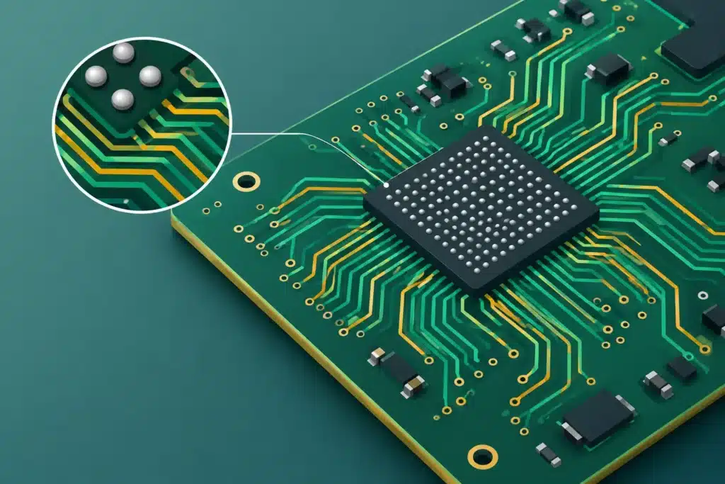
A product may function on the lab bench yet still fail when subjected to real cabling, operational loads, temperature fluctuations, and series production. This PCB redesign case study is based on a typical development cycle where an existing board exhibited recurring EMC issues, unstable power delivery to sensitive circuitry, and unnecessarily high production risks. The solution did not lie in merely repositioning individual components. It required rebuilding the fundamental design architecture so that electrical, mechanical, and manufacturing requirements were addressed as a single, coherent challenge.
The Baseline: A Board with Symptoms, Not a Single Isolated Fault
The existing PCB had been developed under tight schedule constraints. The schematic was largely correct, and the prototype performed its basic functions. However, validation revealed issues commonly intertwined in complex products: emissions hovering near legal limits, susceptibility to external disturbances, sporadic high-speed interface faults, and unit-to-unit variation among prototypes.
It is tempting to address such issues with supplementary decoupling, ferrite beads, or shielding cans. Occasionally, this is the appropriate path. However, when the root causes stem from the layer stackup, return path discontinuities, PDN shortcomings, or component floorplanning, treating the symptoms becomes costly. It also renders the subsequent revision harder to understand and manufacture.
In this project, the objective was not merely to pass a test. The goal was a production-ready redesign grounded in verifiable design rules, a viable fabrication baseline, and a layout topology scalable from prototype to high-volume production.
PCB Redesign Case Study: Identifying Failure Mechanisms First
A redesign should begin with a comprehensive technical audit, not with routing. The original layout, schematics, stackup, component datasheets, test reports, and manufacturing outputs were evaluated collectively. This made it possible to decouple observed symptoms from the underlying physical mechanisms driving them.
For high-speed signals, investigations focused on trace paths, reference plane continuity, via transitions, stub lengths, length matching, and impedance discontinuities. A differential pair is not controlled simply because trace widths appear uniform. If the pair crosses gaps in the reference plane or transitions through vias without dedicated adjacent return paths, discontinuities arise. This increases reflections, common-mode noise, and EMC compliance risks.
The power distribution network was assessed as a PDN, not as a collection of isolated voltage rails. The physical placement and values of decoupling capacitors, via loop inductances, inter-plane capacitance, regulator dynamic responses, and current paths between loads and returns were analyzed concurrently. A capacitor with the correct nominal capacitance provides little benefit if its physical and electrical placement is flawed.
Finally, the layout was evaluated against manufacturing constraints. Fine-pitch devices, BGA fanouts, solder mask bridges, annular rings, copper distribution, and testability access must align with the target fabrication house and the required IPC class. A layout may be electrically optimal yet remain an unviable manufacturing solution.
The Pivotal Decisions: Stackup Architecture and Functional Floorplanning
The primary architectural change did not involve individual traces. It involved a completely restructured stackup featuring defined reference planes and controlled impedances. A stackup must never be selected based simply on a generic layer count. It must be engineered collaboratively with the PCB fabricator, taking into account dielectric materials, copper weights, manufacturing tolerances, impedance targets, and potential HDI structures.
In this case, a clearly defined layer assignments provided superior control. Critical signals were routed on layers with uninterrupted reference planes, power and ground planes were configured to maximize inter-plane capacitance and minimize loop areas, and non-critical routing was diverted away from noise-sensitive circuitry. This eliminated the need for engineering compromises later in the routing phase.
Component floorplanning was then restructured around functional zones. Power supplies, digital processing, high-speed interfaces, analog measurement circuits, and external interfaces were treated as distinct functional blocks with divergent current, noise, and return path requirements. While zoning does not inherently guarantee quiet operation, it provides the topological framework necessary to achieve it.
The connector interface area demanded rigorous discipline. When signals leave the board, the EMC paradigm shifts. Filtering components, ESD protection devices, chassis bonding, and signal return paths must be placed based on actual current loops, not merely what fits at the board edge. Here, the optimal topology depends on enclosure geometry, cable types, grounding topologies, and the applicable regulatory standards.
Addressing Signal and Power Integrity Before Measurement Failures Arise
High-speed designs are frequently scrutinized too late—often only after eye diagrams fail or data links drop packets. In a redesign, establishing strict design constraints prior to detailed routing is far more efficient. This includes specifications for differential and single-ended impedances, maximum via stub lengths, length-matching tolerances, reference plane continuity, and layer-transition rules.
The design utilized short, direct signal paths with tightly coupled return paths. Where layer transitions were unavoidable, ground stitching vias were placed in close proximity to provide a low-inductance return path transition. Though a minor layout detail, with fast edge rates, this can mean the difference between a compliant interface and a persistent radiation source.
On the PDN side, decoupling capacitors were distributed across frequency bands and placed according to their physical proximity to the load. Bulk capacitance located near the regulator handles low-frequency current demands, while localized high-frequency ceramic capacitors placed directly at the IC power pins suppress rapid current transients. There is no universal capacitor matrix. Component values, package sizes, and placements depend on the transient current profile of the IC, rail voltages, layout parasitic inductance, and acceptable ripple limits.
Thermal considerations were integrated directly into the layout. Power components with inadequate copper areas or an insufficient number of thermal vias can suffer degraded operational reliability and altered electrical characteristics. Therefore, a redesign must not merely verify that a component dissipates heat in theory, but must ensure that the thermal dissipation path functions reliably given the actual board thickness, copper weights, and assembly process.
Mitigating EMC Through Layout Geometry and Return Paths
EMC mitigation is rarely an afterthought; it is an inherent property of the layout’s geometry. Large current loops, split reference planes, unfiltered I/O lines, and uncontrolled return currents generate radiated emissions that are difficult and expensive to rectify late in the cycle.
During the redesign, noise sources, coupling mechanisms, and sensitive receivers were evaluated systematically. Switching converters were implemented with compact, minimal high-di/dt loops. Sensitive analog circuits were not merely placed at a physical distance; they were provided with controlled reference planes and well-defined interfaces to the digital subsystems. Physical separation without explicit control over return current paths offers a false sense of security.
Trade-offs, however, must be engineered deliberately. Additional ground vias, filtering stages, and shielding cans may improve EMC performance, but they consume routing space, increase bill-of-materials costs, and constrain assembly tolerances. In designs with aggressive mechanical constraints, each mitigation measure must be justified against its direct risk reduction. A targeted design review is consistently more cost-effective than over-engineering the entire assembly.
Embedding Manufacturing Readiness (DFM/DFA) into the Layout
A PCB redesign is only complete when a fabricator can reliably and repeatedly manufacture the board. Consequently, DFM, DFA, and DFT checks were performed prior to final release. Critical land patterns, solder mask dams, via-in-pad specifications, panelization strategies, fiducials, and test-point accessibility were treated as hard layout constraints, not as administrative checks performed post-design.
For fine-pitch BGAs and high-density interconnect zones, HDI technology was deployed only where it provided tangible engineering value. While blind and microvias reclaim routing channels and improve signal integrity, they also increase fabrication complexity, cost, and vendor qualification requirements. If through-hole vias paired with an additional layer pair achieve a robust design, that may represent the superior solution. The decision hinges on pitch, I/O density, volume requirements, and target reliability metrics.
The production package included unambiguous fabrication drawings, stackup definitions, impedance callouts, assembly documentation, material specifications, and standardized output data. Precise manufacturing requirements eliminate ambiguities between engineering, procurement, and fabrication partners. This shortens manufacturing engineering queries and mitigates the risk of a technically sound layout being fabricated incorrectly.
What an Engineering Team Should Gain from a Redesign Process
The true value of a PCB redesign extends beyond receiving the next revision of Gerber or ODB++ data. A well-executed redesign leaves the engineering team with defensible design decisions: why the stackup was selected, which impedances are critical, how grounding and chassis bonding are partitioned, and which manufacturing limits apply.
For engineering teams facing critical deadlines, engaging a senior specialist shortens the cycle from failure analysis to a fully realized layout, ensuring that analysis, floorplanning, routing, and fabrication inputs proceed in lockstep. At Wise Choice Support, you maintain direct communication with the same PCB specialist throughout the entire scope of work. This accelerates technical decision-making and ensures clear accountability.
When redesigning an existing circuit board, the most critical question is not how quickly a set of changes can be completed. The question is whether every modification systematically moves the product closer to verified signal integrity, robust power delivery, EMC compliance, and scalable production yields. That is where a redesign transitions from a simple revision into a permanent engineering solution.