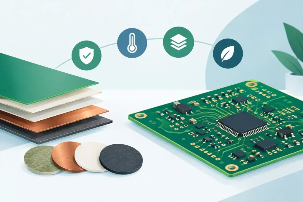
A BGA footprint can appear straightforward in a schematic while becoming the most constraining factor of the entire PCB layout. This guide to BGA escape routing focuses on the decisions that determine whether the component can be routed, manufactured, and operate reliably—even when the design incorporates high-speed interfaces, sensitive power rails, and tight mechanical tolerances.
Escape routing is not merely the mechanical task of routing traces out between pads. It is the foundational geometry that dictates layer count, via technology, return paths, PDN behavior, assembly yield, and rework viability. When the via strategy is decided late in the process, the result is frequently a costlier stackup, compromised impedances, or a layout producible by only a handful of specialized fabricators.
Start with the BGA Geometry—Not the Routing Tool
Pitch, ball diameter, pad type, and the number of rows define the feasible routing window. At a 1.0 mm pitch, standard dogbone escape routing utilizing through-hole vias is generally viable, depending on pad and trace design rules. At a 0.8 mm pitch, routing space constricts rapidly, particularly when breaking out multiple internal layers. At 0.65 mm and below, microvias, via-in-pad, or a hybrid approach typically become mandatory.
Relying solely on pitch as the deciding metric is an oversight; the BGA pinout is equally critical. If high-speed differential pairs, DDR byte lanes, clock lines, analog references, and multiple power domains are distributed without routing foresight, an escape that is geometrically feasible may still prove electrically defective. High-performance layout engineering therefore begins with rigorous pinout analysis: Which signals demand the shortest, most symmetrical paths? Which nets can tolerate layer transitions? Where must decoupling capacitors reside? And which areas must be allocated for dedicated power and ground vias?
Guide to BGA Escape Routing: Define the Via Strategy Early
Via technology must align with electrical constraints, target production volumes, and the capabilities of the chosen PCB fabricator. There is no single universal solution.
Dogbone Routing with Plated Through-Hole Vias
Dogbone routing places the via directly outside the BGA pad, connecting the pad and via with a short trace segment. This methodology is well-understood, cost-effective, and highly robust in manufacturing when pitch and design rules permit. It is typically well-suited for industrial designs with a pitch of 1.0 mm or greater.
The primary drawback is board area consumption. The via and breakout trace occupy the routing channel between solder balls, and the via stub from a through-hole via can severely degrade high-speed serial interfaces. When a 10 Gbps or faster signal traverses a via featuring a long, unused stub, reflections and insertion loss become hard performance limiters. Backdrilling can mitigate this issue, but adds process complexity and fabrication cost.
Blind Microvias and HDI Architecture
Laser-drilled microvias connecting outer layers to adjacent inner layers enable a considerably more compact escape. This frees up internal routing layers and allows layout designers to accommodate finer pitches without resorting to excessively thin traces. For high-density FPGAs, processors, RF modules, and advanced SoCs, an HDI approach is frequently the correct technical path.
However, microvias demand strict discipline regarding stackup architecture and fabricator capability specifications. Aspect ratios, copper filling, stacked versus staggered configurations, and IPC compliance must align directly with the selected manufacturing process. A stacked microvia configuration saves horizontal board space but introduces tighter tolerances for filling, layer-to-layer registration, and overall reliability. For products subjected to thermal cycling, sustained vibration, or extended operating lifespans, this selection must never be made solely on routing density.
Via-in-Pad, Filled and Capped Vias
Via-in-pad is required when every BGA pad must be fully utilized for routing channels, or when the thermal and electrical performance of the component necessitates minimal inductance paths directly to internal planes. Vias placed inside solder pads must typically be filled and planarized (capped) to prevent solder wicking into the barrel during reflow. Without appropriate processing, the assembly is prone to voiding, insufficient solder joints, and degraded assembly yield.
While this approach delivers high routing density and minimized trace lengths, it incurs substantial fabrication overhead. It must be justified by fine pitch, signal integrity, thermal dissipation, or layer-count reduction—not adopted merely as a preference for advanced technology. In many cases, a 1.0 mm pitch BGA with moderate interface requirements will yield a more robust and cost-efficient design using a well-controlled dogbone strategy.
Stackup and Return Paths Must Precede Fanout
BGA escape routing cannot be evaluated independently of the PCB stackup. When a signal leaves the BGA on an outer layer and transitions to an internal signal layer, a continuous reference plane must reside immediately adjacent to the signal conductor. Failing to provide this breaks the return path, causing the via transition to introduce parasitic inductance, mode conversion, and severe EMC vulnerabilities.
For differential pairs, the objective extends beyond maintaining parallel trace geometries. The pair must exhibit tightly managed differential impedance throughout its entire path, including pad exits, via transitions, and any localized neck-down regions. Within dense BGA breakout fields, trace widths may be narrowed relative to the rest of the board. This is acceptable provided the transition is short, controlled, and incorporated into comprehensive impedance calculations. Replicating legacy design rules from previous layouts without revalidation is unacceptable practice.
When routing transitions occur across reference planes, stitching vias must be placed in close electrical proximity to the signal vias. This is vital for fast single-ended nets and high edge-rate differential pairs. A ground return via is not a cosmetic layout addition; it serves as an integral part of the signal loop and the electrical circuit.
Power Distribution Requires Dedicated Space in the Escape Field
The most demanding elements of the PDN converge directly beneath and around the BGA: low-voltage processor core rails, I/O supplies, sensitive PLL rails, and dedicated analog domains. If the escape routing consumes all available pads and routing channels for signal traces, insufficient capacity remains for low-inductance power and ground vias. The consequence is elevated via inductance, poor decoupling efficacy, and severe transient voltage drop during dynamic load switching.
Decoupling capacitors must be connected via short, wide, and symmetrical current loops. In practice, this means capacitor placement, via-pair assignments, and relevant reference plane assignments must be designed concurrently with the BGA fanout. A capacitor placed in close physical proximity to the component provides negligible decoupling benefit if current must traverse long, inductive traces and multiple redundant vias.
For large-pin-count BGAs, dedicating predefined escape zones exclusively to power and ground distribution is often necessary. While this may reduce the number of usable signal channels on an individual routing layer, it yields a measurably more stable and robust hardware design. High routing density must never be conflated with high electrical performance.
Design Rules Must Be Fabricator-Specific
Minimum trace width, spacing, annular ring size, solder mask clearance, and microvia dimensions must never rely on theoretical assumptions. They must be coordinated directly with the designated PCB fabricator or matched strictly to an established process class available across multiple qualified manufacturing partners.
Solder mask definition between BGA pads requires special scrutiny. At fine pitches, solder mask webs (slivers) can become excessively narrow, forcing fabricators to either mandate Solder Mask Defined (SMD) pads or eliminate the mask web entirely. Both approaches alter the effective copper geometry, solder volume, and assembly risk profiles. PCB fabrication capabilities and assembly processes must therefore be evaluated concurrently.
IPC Class 2 and Class 3 impose fundamentally different mandates regarding documentation, process tolerances, and acceptable defect criteria. However, specifying a manufacturing class designation does not resolve an inherently flawed footprint or an overly aggressive via implementation. The layout must be verifiable against documented fabrication rules, with all critical design tolerances explicitly delineated in the fabrication and assembly data package.
Verify Critical Transitions Prior to Release
A visually coherent BGA fanout is not inherently sound from an electrical or manufacturing perspective. Prior to design freeze and release, critical nets must undergo thorough design reviews focusing on via stub lengths, reference plane discontinuities, target impedance profiles, pair symmetry, length/phase matching, and return stitching via placement. For ultra-high-speed interfaces, full 3D electromagnetic field extraction of the BGA breakout and via transitions is strongly warranted, especially when manufacturer guidelines do not account for the specific layer stackup.
Concurrently, the DFM review must validate padstacks, copper plating distribution, solder mask constraints, microvia reliability structures, and line-of-sight access for AOI, X-ray inspection (AXI), and rework procedures. BGA solder joint failures are difficult to identify post-assembly; consequently, process risks must be eliminated in the design phase, not diagnosed after the initial reflow run.
At Wise Choice Support, BGA escape routing is engineered as an integrated facet of the overall PCB architecture—from pinout mapping and layer stackup synthesis to signal integrity, PDN performance, EMC mitigation, and production data release. This rigorous approach transforms a complex breakout into a fully verified, production-ready hardware platform, ensuring compromises do not surface downstream on the test bench or in volume manufacturing.
When selecting your next BGA component, the fundamental question is not simply whether it can be routed. The real question is whether it can be routed with controlled impedance, low PDN inductance, realistic manufacturing tolerances, and the operational stability required throughout the entire product lifecycle.