When sizing decoupling capacitors, the primary question is not simply how many microfarads can physically fit on the PCB. The critical factor is whether the PDN can deliver the transient current to each IC without unacceptable voltage drops, resonances, or noise propagating into the rest of the system. An arbitrary collection of 100 nF capacitors may look adequate in the schematic, yet still result in an unstable product on the lab bench.
For high-speed, RF, FPGAs, processors, ADCs, and fast switch-mode loads, decoupling must be addressed as an integral part of power integrity design. Capacitor value, package, DC bias, parasitic inductances, stackup, via geometry, and placement relative to power pins all interact. A failure in any one of these disciplines can render a correctly chosen capacitor electrically irrelevant.
Size Decoupling Capacitors Based on PDN Requirements
A practical starting point is determining the target PDN impedance. This is calculated as:
`Z_target = ΔV / ΔI`
Here, ΔV represents the maximum allowable voltage ripple on the rail, and ΔI is the expected transient load step. If a 1.0 V core supply is permitted to deviate by 30 mV during a 3 A transient step, the target impedance is 10 mΩ. The PDN must therefore maintain its aggregate impedance below 10 mΩ across the entire frequency range where the load draws energy.
This is a design target, not a guarantee that a single capacitor will resolve the requirement. At low frequencies, energy is typically supplied by the voltage regulator and bulk capacitance. In the mid-frequency range, local capacitor banks supply the energy. At high frequencies, package inductance, power-ground plane coupling, and the IC’s on-die capacitance dominate. These transition boundaries depend on the regulator's control loop, the IC's transient profile, and the physical implementation.
Start with the Load’s Actual Current Profile
Datasheet recommendations—such as 10 x 100 nF and 2 x 10 µF—serve merely as starting points, not complete PDN designs. This is especially true when a reference design utilizes a different stackup, an alternative regulator, fewer power planes, or larger physical distances between the IC and the power source.
For critical rails, the current profile must be evaluated in both the time and frequency domains. An FPGA can exhibit sharp current transients during state transitions, clock gating changes, or I/O switching. An ADC may draw periodic current pulses that couple directly into analog noise floors. An RF power amplifier can generate pulsed loads that modulate the supply rail, adversely affecting spectral purity and EMC compliance.
Once the transient parameters are known, the required ideal capacitance can be estimated using:
`C = ΔI × Δt / ΔV`
While this calculation is useful for estimating total energy storage requirements, it ignores ESR and ESL. Under fast edge rates, inductance often becomes the limiting factor long before the nominal capacitance is depleted. Consequently, this calculation must always be augmented by an analysis of impedance versus frequency and the specific physical layout loop.
Nominal Capacitance Tells Only Part of the Story
A ceramic MLCC does not deliver its marked nominal capacitance under all operating conditions. Dielectric characteristics, DC bias, temperature, aging, and manufacturing tolerances degrade effective capacitance. A 10 µF X5R capacitor on a low-voltage rail can lose a significant portion of its capacitance when subjected to a DC operating voltage. This is not inherently problematic if derated correctly, but it becomes critical when a design relies solely on nominal ratings.
ESR can be beneficial within specific limits to dampen resonant peaks, but excessive ESR induces larger voltage drops during dynamic load steps. ESL is determined both by the internal construction of the component and by its mounting geometry. An 0402 package typically exhibits lower ESL at high frequencies than a 1206 package; however, the smaller package offers lower maximum capacitance and reduced tolerance to mechanical stress. Selection depends strictly on the target frequency range and mechanical manufacturing constraints.
Every capacitor exhibits a self-resonant frequency (SRF). Below this resonance, it behaves capacitively; at resonance, impedance reaches its minimum; above resonance, inductive behavior dominates. Therefore, combining random capacitor values does not inherently yield a wide, low-impedance profile. Paralleling disparate capacitance values can create anti-resonance peaks where impedance rises sharply. This is a primary reason why an unverified capacitor network can fail within a narrow, critical frequency band.
An optimized solution does not necessarily require capacitors spanning multiple decades of values. Frequently, a controlled combination of fewer, well-selected values, appropriate package sizes, and adequate damping yields more predictable performance. Simulation incorporating manufacturer S-parameters—including ESL, ESR, and DC bias derating—is the definitive method for validation.
Layout Determines Whether the Capacitor Functions
A decoupling capacitor must be routed such that current traverses the minimal loop area between the IC power pin, the capacitor, and the reference return plane. Distance cannot be assessed purely in terms of top-layer trace length. Vias, dielectric thickness to reference planes, pad geometry, and the return current path all form part of the critical loop.
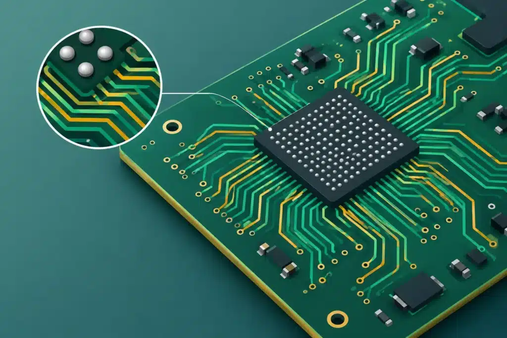
For BGA components, this necessitates a deliberate fanout strategy. Mounting capacitors on the PCB backside can be effective, provided via stubs, via pair spacing, and plane transitions are strictly managed. However, a capacitor placed directly beneath a BGA is not inherently superior to one on the top layer if the latter provides a lower-inductance, shorter electrical path. Decisions must be governed by loop inductance, not physical proximity alone.
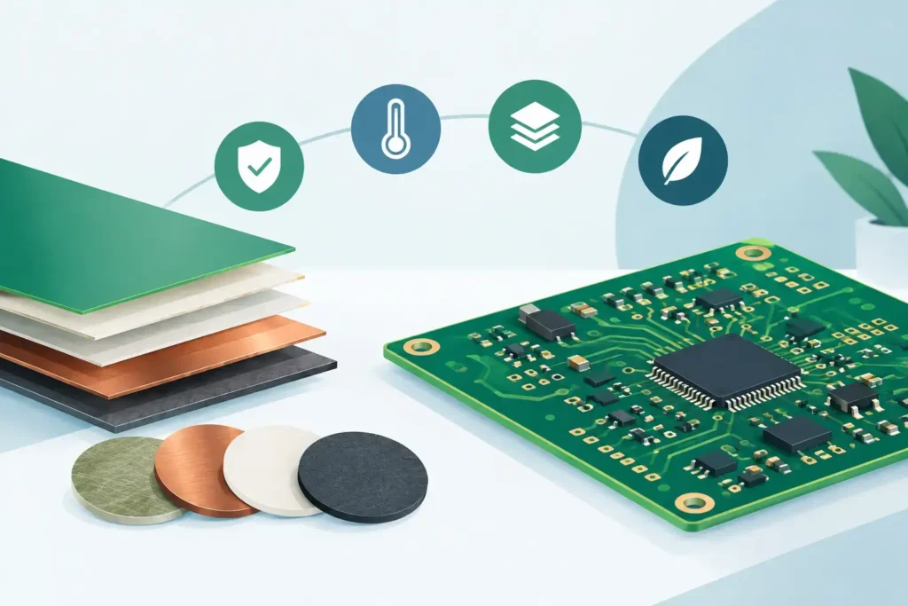
Power and ground plane pairs separated by thin dielectrics provide significant distributed interplane capacitance and ultra-low parasitic inductance. This mechanism becomes dominant at frequencies where discrete surface-mount capacitors lose effectiveness. Consequently, a stackup featuring closely coupled plane pairs adjacent to the component layer can improve PDN performance more substantially than adding discrete capacitors to a poorly planned layer stack.
Avoid routing power through long, narrow traces to a capacitor bank and subsequently to the load. Furthermore, avoid shared vias that force multiple high-frequency return currents through the same inductive constraint. Shared via structures increase mutual impedance and can induce cross-domain noise coupling between critical sub-circuits, such as digital cores, SerDes transceivers, analog references, and RF rails.
Bulk Capacitance, Local Decoupling, and Regulators Must Be Coordinated
Bulk capacitors must supply energy over longer durations, spanning the regulator's response time and lower-frequency load variations. These are typically placed adjacent to the regulator output or at the entry point of a power island, where thermal dissipation and current density can be properly managed. Local MLCCs placed close to the IC pins manage immediate, high-frequency current demands.
Treating the voltage regulator, its output capacitors, and the downstream load decoupling as isolated subsystems is a fundamental design flaw. Switch-mode regulators impose strict requirements on output capacitance, ESR, and stability margins. Introducing additional downline capacitance or modifying the impedance profile can destabilize the control loop. For noise-sensitive rails, regulator Bode plots, output filter networks, and transient load spectra must be evaluated within a unified PDN analysis.
Ferrite beads require the same rigorous evaluation. While effective at isolating noise between supply domains, they form resonant LC tank circuits when combined with capacitive decoupling on either side. A ferrite bead is not an arbitrary noise remedy. In many applications, low-value series damping resistors, controlled RC networks, or distinct plane partitioning provide superior, resonance-free isolation.
Verify the PDN Before and After Layout
Prior to layout implementation, target impedance, capacitor types, package geometries, plane pairings, and regulator topologies should be clearly established as engineering constraints. Following placement and routing, the PDN must be post-layout verified incorporating actual parasitic extraction. This is particularly vital for low-voltage, high-current designs, high-speed digital interfaces, and assemblies subject to stringent EMC requirements.
Empirical verification requires precise methodology. Standard oscilloscope probes with long ground leads introduce significant parasitic loop inductance, displaying false ringing that does not exist at the IC silicon. Utilize low-inductance ground springs, matched coaxial probes, and measure as close to the load die as physically possible. For complex mission-critical designs, VNA-based PDN impedance measurements and correlation against pre-layout simulations are mandatory.
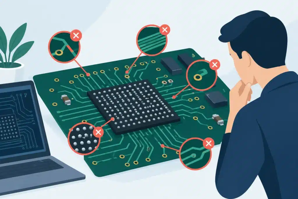
Look out for system symptoms that are commonly misdiagnosed: intermittent resets, bit errors under heavy computational load, elevated phase jitter, reference rail degradation, radiated emissions failures, or sensitivity to thermal changes and cabling configurations. While these failures can stem from various sources, an irregular PDN impedance profile with anti-resonant peaks or insufficient local decoupling is very frequently the root cause.
The correct decoupling methodology is the one proven to keep power supply ripple and noise within component margins in the completed layout under real-world operating conditions. When design margins are tight, component sizing, stackup synthesis, and physical placement must be executed as a unified engineering discipline—not fragmented across schematics, PCB layout, and post-production troubleshooting. Engaging in a targeted PDN review early in the design cycle prevents costly layout iterations and critical validation failures.