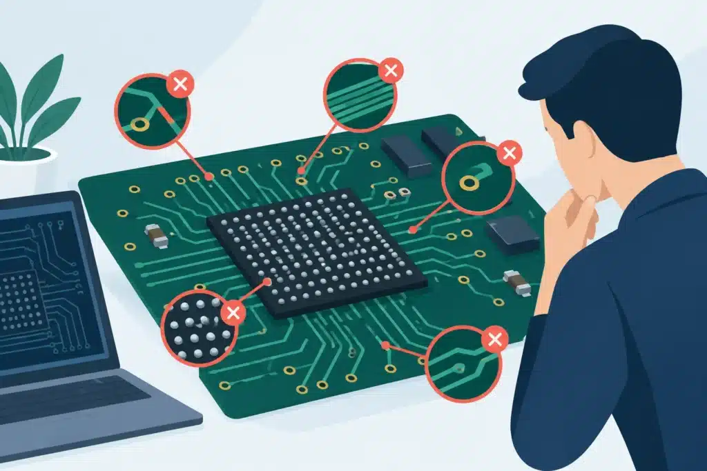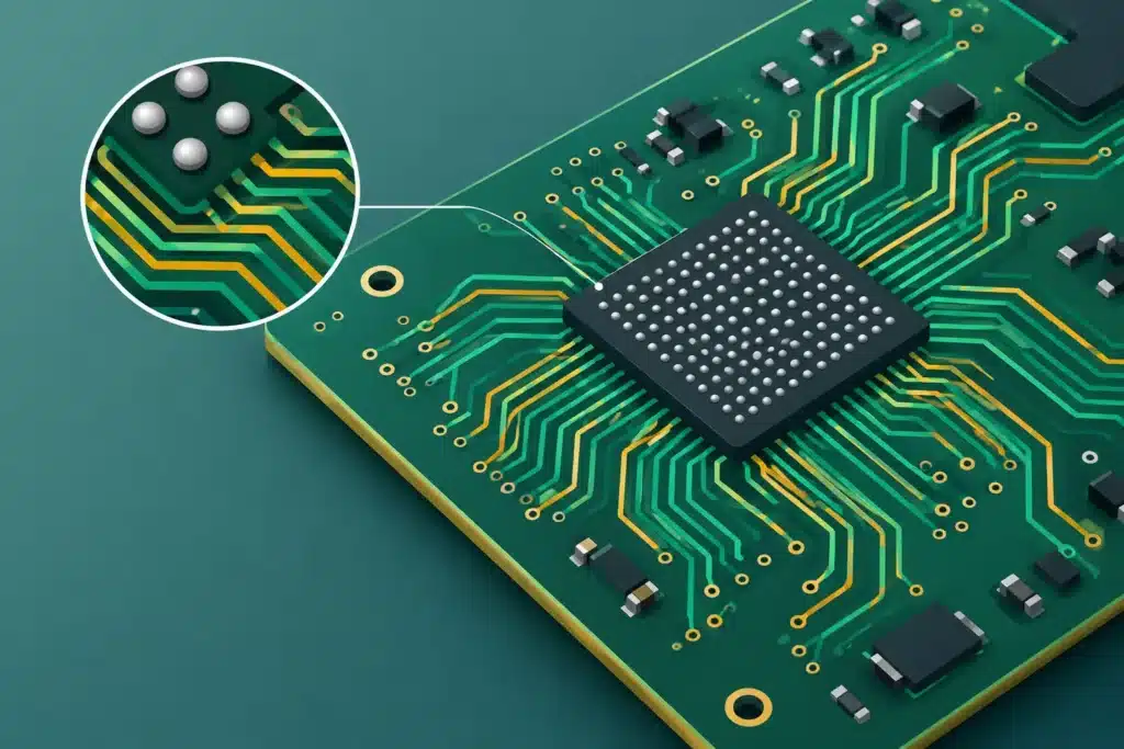
A printed circuit board rarely fails due to a single incorrect material parameter. The issue typically arises when the laminate is selected based on a generic FR-4 designation, while real-world requirements are dictated by frequency, temperature, voltage levels, EMC, stackup, and the manufacturing process. This PCB material selection guide is based on the parameters that determine whether a design remains stable in the field, or whether it will later require troubleshooting, redesign, and requalification.
For simple, low-frequency products with limited thermal stress, a standard laminate can be a sensible choice. However, when the design incorporates high-speed digital interfaces, RF, high power, dense BGAs, HDI, or extended operational lifetime requirements, material selection becomes an engineering decision—not a procurement decision. The material directly impacts signal integrity, PDN, EMC, mechanical stability, and manufacturing yield.
PCB Material Selection Begins with the Real-World Operating Stresses
The right question is not: Which FR-4 material should be used? The right question is: Which electrical, thermal, mechanical, and manufacturing stresses must the board withstand throughout its entire lifecycle?
A 28 Gbps link, a radar front-end, a motor drive, and a medical instrument can all be built on multilayer PCBs, but their laminate requirements are fundamentally different. High-speed signals require a stable dielectric constant and low loss. Power electronics demand control over heat dissipation, copper thickness, and thermal cycling. RF designs require consistent material data at the actual operating frequency. In environments subject to vibration, humidity, vacuum, or wide temperature swings, z-axis expansion, resin content, and the material's proven reliability become critical.
Consequently, material selection should be established concurrently with the stackup, impedance requirements, and component strategy. It is too late to discuss laminates once the layout is completed, vias are placed, and the fabricator's capabilities are already pushed to their limits.
The Electrical Parameters Governing Signal Integrity
Dk Is Only Actionable When the Measurement Conditions Are Known
The dielectric constant, Dk, is used to calculate impedance and signal propagation velocity. However, a single datasheet value is insufficient. Dk depends on the test method, frequency, resin content, glass weave, and frequently the orientation of the signal trace relative to the weave pattern.
If a controlled impedance trace is calculated using a nominally incorrect Dk value, the resulting impedance can deviate noticeably from the target. At moderate digital speeds, the tolerance budget may absorb this deviation. At high data rates, tight margins, or RF frequencies, this is rarely the case. Here, stackup data must originate from the specific fabrication facility and the concrete laminate system, including copper foil profile, prepreg pressed thicknesses, and the glass style employed.
The glass weave effect warrants particular attention in high-speed serial interfaces. A differential pair can experience different effective Dk values across the two conductors if one trace runs over glass bundles and the other over resin pockets. This can induce skew and degrade the eye diagram. Solutions include spread-glass materials, routing at an angle (zig-zag routing), or adjusting the stackup. The optimal approach depends on data rates, board geometry, and fabrication capabilities.
Df Determines How Much of the Signal Dissipates as Heat
The dissipation factor, Df or loss tangent, characterizes the dielectric loss of the material. The higher the frequency and the longer the transmission line, the greater the impact of Df. A material with relatively high loss may function reliably in a general microcontroller application, but prove unacceptable in long backplane links, high-frequency RF, or data center hardware with stringent link budgets.
Low-Df materials are not automatically the optimal choice. They can be more expensive, impose different processing requirements, and constrain fabricator material sourcing. If the channel length is short and the receiver provides sufficient equalization margin, a standard material may be both technically and economically sound. The decision must be based on a comprehensive channel budget, not simply the desire for the lowest possible number on a datasheet.
Thermal Properties Extend Beyond Tg
Glass transition temperature, Tg, is often used as a quick indicator of a laminate's thermal robustness. A high Tg is relevant, but it does not alone describe how the material behaves during assembly soldering, normal operation, and repeated thermal cycling.
CTE in the z-axis is critical, particularly with BGAs, fine-pitch components, high layer counts, and HDI structures. When the PCB heats up, the material expands. Excessive z-axis expansion places mechanical stress on vias, barrel plating, and solder joints. The risk increases with board thickness, the number of thermal cycles, and architectures featuring blind and buried vias.
Decomposition temperature, Td, and time-to-delamination provide critical data regarding the material's endurance through specific reflow soldering profiles. This is particularly relevant when the board must undergo multiple reflow passes, contains heavy copper planes, or requires rework. A PCB may pass electrical testing immediately post-production yet suffer from a compromised operational lifespan if the material was overstressed during processing.
For power and LED designs, thermal conductivity must also be evaluated. Standard laminate conducts heat poorly compared to copper and metal-core substrates. Frequently, the most effective improvement is not an exotic material, but a targeted combination of copper planes, thermal vias, optimized component placement, and realistic thermal analysis.
Copper Foil Type and Surface Roughness Impact Both Insertion Loss and Manufacturing
Copper is not simply copper. Foil type, thickness, roughness, and treatment significantly influence high-frequency loss, etching precision, adhesion, and current-carrying capacity. At high frequencies, current concentrates near the copper surface due to the skin effect. A rough profile effectively lengthens the signal path and increases insertion loss.
Very low-profile (VLP) copper can reduce loss, but introduces trade-offs regarding peel strength and processing windows. This must be evaluated in accordance with the laminate manufacturer's guidelines and the chosen fabricator. Similarly, heavy copper must be selected with a clear understanding of mechanical and manufacturability implications. Thicker copper aids current capacity and heat transfer, but alters impedance calculations, necessitates larger trace spacing, and complicates the reliable fabrication of fine features.
Stackup and Material Selection Cannot Be Decoupled
A theoretically superior material cannot compensate for a poorly conceived stackup. Signal layers require well-defined reference planes, and the dielectric distance to these planes must align with impedance targets, loss requirements, and manufacturing tolerances. For high-speed signals, return currents require an uninterrupted, controlled return path. A low-Df laminate cannot correct for broken reference planes, poorly transitioned vias, or an excessively high-impedance PDN.
The same holds true for EMC. While material characteristics influence field propagation, loss, and cavity resonances, EMC performance is largely governed by layer distribution, plane integrity, decoupling strategies, cable interfaces, and mechanical shielding. Material selection must therefore be integrated into a comprehensive design review that evaluates the schematic, layout, stackup, and manufacturing baseline as a cohesive whole.
Manufacturing and Sourcing Must Be Addressed from Revision Zero
The most advanced laminate becomes a liability if it entails extended, volatile lead times or single-source dependency on a fabricator that cannot support production volume. Clear visibility is required regarding material availability, approved alternative laminates, minimum order quantities (MOQs), and compliance documentation.
IPC class, CAF resistance requirements, via aspect ratios, sequential lamination cycles, and test strategies also direct the choice. An HDI board utilizing microvias demands a distinct material discipline compared to a conventional through-hole multilayer board. In aerospace, defense, and medical electronics, traceability, lot control, and documented process histories can be as critical as nominal electrical specifications.
At Wise Choice Support, material selection is treated as an integral component of production-ready engineering. Material, stackup, impedance modeling, DFM, and fabrication capabilities must be verified and aligned prior to layout freeze. This eliminates the risk of discovering invalid technical assumptions during initial prototyping.
A Practical Decision Framework
Begin by defining the operating environment, operational lifespan requirements, frequency bands, data rates, voltage levels, and thermal loads. Next, define the stackup, layer functions, and impedance requirements in collaboration with the targeted PCB fabricator. Only then does it make sense to benchmark specific laminate systems against Dk, Df, Tg, CTE, copper foil profiles, and process compatibility.
For complex boards, board space must be allocated for physical validation. This includes impedance test coupons, material verification coupons, TDR measurements, thermal profiling, or RF characterization structures. An assumption is not a specification until it can be empirically measured and verified on the fabricated printed circuit board.
The most cost-effective PCB material is not necessarily the least expensive per square meter. It is the material that delivers the necessary electrical margins, reliably withstands the actual fabrication process, and ensures stable field performance—preventing costly redesigns when operational margins diminish.