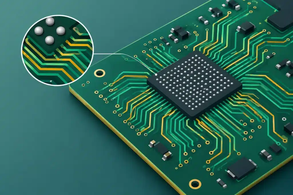
An example of an optimized power supply layout does not begin with where there is space for the regulator. It begins with the current paths. A switch-mode power supply can feature a fully validated schematic yet still fail EMC testing, introduce jitter into sensitive circuits, or trigger unexpected resets if high-speed current loops and return paths are treated as standard routing.
In complex PCBs, the power supply is integral to overall signal integrity, EMC performance, and thermal management. This is especially true in designs incorporating FPGAs, ADCs, RF stages, high-speed interfaces, or high currents, where minor layout deficiencies can escalate localized noise into system-wide failures.
A practical example of an optimized power supply layout
Consider a six-layer PCB with a 12 V input and a synchronous buck converter delivering 5 V at up to 10 A to digital circuitry. Downstream rails of 3.3 V, 1.8 V, and low-noise analog voltages are subsequently generated from this 5 V rail. The converter is positioned in close proximity to the power input and nearer to high-draw 5 V loads than to sensitive analog sections.
The core layout principle is straightforward: minimize the high-frequency input loop area. The input ceramic capacitors must be placed directly across the regulator's VIN and PGND pins, utilizing short, wide copper traces and multiple ground vias placed immediately adjacent to the capacitor ground pads. A long 12 V trace between the capacitor and IC is unacceptable, regardless of trace width, as loop inductance typically dominates over DC resistance.
The switch node between the regulator and the inductor must remain compact. The copper pour must provide adequate area to handle current and thermal dissipation without becoming an efficient radiating antenna. Due to high dV/dt, this node must be routed well clear of the feedback network, connectors, sensitive signals, and internal layers with parallel signal routing.
Following the inductor, output capacitors are positioned immediately adjacent to the inductor's load terminal. Their dual function is to minimize output voltage ripple and supply local, high-speed current transients. If the load is an FPGA or processor, supplementary bulk and ceramic decoupling must reside directly at the load, not merely at the converter. A 5 V plane distributes power but cannot replace local decoupling for dynamic loads.
Stackup and return paths must support the PDN
In this design, Layer 2 functions as a solid, continuous GND plane, establishing a low-inductance reference plane for the regulator, decoupling capacitors, and top-layer digital signals. Layer 3 can be allocated for 12 V and 5 V distribution, while remaining internal layers are reserved for secondary rails, signal routing, and supplementary GND planes as required.
A continuous ground plane is generally superior to a split plane, though specific exceptions exist. High-voltage isolation, regulatory safety standards, or specialized analog domains may necessitate physical boundaries. The exact strategy depends on clearance rules, noise-coupling mechanisms, and component grounding topologies. Crucially, high-frequency currents must always have an uninterrupted return plane directly beneath the forward path.
A common design flaw is splitting the ground plane beneath the regulator to segregate analog and digital grounds. This frequently forces return currents around the perimeter of the split, increasing loop area, radiated emissions, and ground reference bounce. Analog precision is rarely achieved through arbitrary ground cuts; it requires meticulous component placement, filtering, controlled current paths, and physical isolation of noisy nodes from sensitive circuitry.
Feedback must be sensed where voltage regulation is critical
The feedback trace from the 5 V output must be routed as a dedicated Kelvin connection taken after the inductor, preferably directly across the primary output capacitor. It must never be tapped arbitrarily from an active 5 V plane where dynamic load currents generate IR drops. Otherwise, the converter regulates accurately, but at the wrong physical location.
The feedback network must be positioned away from the switch node and the inductor, referenced to a quiet ground as specified in the regulator's datasheet. Many topologies require analog ground and power ground to tie locally beneath or adjacent to the IC; however, internal architectures differ. Applying a generic star-ground scheme without evaluating the component’s internal architecture compromises stability.
If the regulator utilizes external loop compensation, component placement is as critical as component values. Excessive trace lengths to compensation resistors and capacitors readily pick up switching noise, degrading loop stability. This vulnerability typically manifests as load-dependent ripple, erratic overshoot, or unit-to-unit variation between PCB revisions.
Copper dimensioning for DC losses and thermal dissipation
Carrying 10 A on a 5 V rail requires far more than merely widening a trace. Copper weight, trace geometry, via arrays, thermal choke points, and actual current density must be analyzed holistically. A copper pour that visually appears sufficient in CAD can develop severe localized current density bottlenecks at narrow transitions, dense via fields, or component pads.
In high-reliability practice, parallel vias are implemented at layer transitions to minimize parasitic resistance and loop inductance. Sizing the via count must not rely solely on nominal current ratings; thermal rise, manufacturing tolerances, solder voiding in via-in-pad applications, and dynamic current distribution must be factored in. At elevated currents, a poorly planned layer transition can become the primary thermal hotspot.
Thermal vias placed beneath the regulator’s exposed pad must tie directly into appropriate copper pours and internal reference planes. However, their placement and diameter must avoid solder wicking during reflow, which compromises joint integrity. Footprint design, stencil aperture strategy, solder profiles, and PCB fabrication capabilities must be aligned. A production-ready layout encompasses both electrical integrity and manufacturability.
Decoupling placement based on frequency and current path
Decoupling capacitors must not be treated as a lumped pool distributed haphazardly across the layout. Each capacitor has a distinct role within the PDN. Low-value ceramic capacitors suppress fast, high-frequency transients directly at the IC supply pins, whereas higher-capacitance components support lower-frequency load steps and localized energy storage.
Component efficacy is governed by total ESL and mounting geometry. A 100 nF capacitor placed 30 mm away from an FPGA power pin offers negligible attenuation at high frequencies. Short trace lengths, wide pads, direct connections to the GND plane, and vias placed immediately at the pads yield far greater improvements than simply adding more distant decoupling capacitors.
When designing multi-rail systems, power sequencing and turn-on profiles must be integrated into the architecture early. A buck converter that exhibits standalone stability can cause rail droop or trip protections if downstream converters, large capacitive loads, or hot-swap events disrupt power ramp-up. Startup performance must be validated against soft-start parameters, current limits, and load requirements.
Suppress EMC at the source, not with retrofitted filters
Input filters, ferrite beads, and common-mode chokes are frequently required—especially in cabled systems—yet they cannot compensate for an inadequate power layout. If the primary hot loop is oversized or the switch node couples capacitively into adjacent copper, switching noise will bypass external filters and propagate through the system.
An effective EMC strategy begins by isolating noise mechanisms: high di/dt within the input loop, high dV/dt on the switch node, parasitic ringing, and common-mode currents targeting cabling or the chassis. Component placement, stackup architecture, plane shielding, and filtering are then tailored to the specific coupling modes present.
Prototype validation is essential, but it delivers maximum value when the layout is established on engineered current paths. Switch-node probing, ripple measurements using proper tip-and-barrel techniques, thermal imaging, and conducted emissions testing must be used to validate engineering calculations, rather than to troubleshoot an unstructured layout.
Required documentation prior to design release
Prior to manufacturing release, the power supply layout must be fully documented to ensure hardware and manufacturing teams can make reliable engineering decisions. The release package should encompass:
- Defined current paths, return current geometries, and critical high-frequency loop boundaries.
- PDN parameters, decoupling strategy, and maximum IR drop calculations under full load.
- Thermal analysis of the regulator, inductor, via transitions, and copper distribution.
- EMC risk assessments, critical isolation/clearance regions, and prototype validation test plans.
An optimized power supply layout is evident in more than clean copper polygons. It reflects deliberate design choices regarding current flow, reference continuity, thermals, loop stability, and manufacturing yield. Implementing these controls before routing translates to copper dramatically reduces costly design respins. This senior-level PCB expertise makes the fundamental difference between a board that merely powers on and a production-grade assembly engineered for mission-critical reliability.