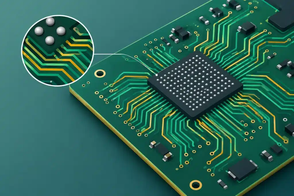
A BGA with hundreds or thousands of solder balls leaves very little room for assumptions. Five BGA routing errors recur consistently in design reviews—often in layouts that appear clean and manufacturable on paper. The problem only surfaces later: during bring-up, inside the EMC chamber, during temperature cycling, or as unacceptable yield loss at the manufacturer.
BGA routing is not merely a matter of breaking out all nets to the perimeter. Fanout, layer stackup, via architecture, return paths, the PDN, and fabrication processes must function as a single, coherent system. This is especially true for FPGAs, processors, DDR, SerDes components, and advanced mixed-signal designs, where a local layout decision can have consequences across the entire PCB.
Five BGA Routing Mistakes That Must Be Addressed Early
1. Selecting Fanout Before Finalizing Stackup and Fabricator Capabilities
It is tempting to begin escape routing as soon as the footprint is placed. However, the choice between dogbone fanout, via-in-pad, staggered microvias, or a hybrid combination depends on the actual layer stackup, BGA pitch, required trace widths, and the manufacturer's verified capabilities.
A 0.8 mm pitch BGA can often be routed using conventional through-hole vias and a sound layer strategy. At 0.5 mm and below, the scenario changes rapidly. Here, HDI with laser-drilled microvias may be necessary, but that does not mean every pad requires via-in-pad. The optimal solution depends on breakout density, the required number of signal and power layers, impedance requirements, and targeted production economics.
The mistake arises when the layout relies on generic minimum design rules rather than direct dialogue with the PCB fabricator. The result is often a board that either cannot be manufactured using the intended technology or requires an unnecessarily expensive process. Therefore, the stackup must be finalized before freezing the BGA fanout. Dielectrics, copper weights, drill types, annular rings, capture pads, and sequential lamination are not details that can be postponed to the final phase.
2. Implementing Microvias Without Regard for Reliability and Stacking
Microvias resolve routing density constraints, but they do not eliminate physical limitations. Stacked microvias in particular require rigorous evaluation regarding via filling, copper plating, laser drilling parameters, and thermal stress. If a via structure is chosen solely to eliminate a routing layer, it can become the primary point of failure in the product.
It is essential to distinguish between a laboratory prototype, an industrial product, and a high-reliability system for mission-critical sectors such as medical devices, defense, or aerospace. A via architecture that functions across a small batch of bench prototypes is not inherently suitable for series production or long-term operational life under mechanical vibration and thermal cycling.
Blind vias and staggered microvias frequently offer a superior compromise among routability, cost, and operational reliability compared to aggressively stacked vias. However, this depends on breakout density and the required interconnect path through the stackup. The decision must be based on the fabricator's qualified process window and the product’s mission profile—not merely on what the CAD tool allows.
3. Disrupting the Return Path Beneath the BGA
High-speed signals do not simply travel along copper traces. The return current seeks the path of least impedance through the nearest reference plane, and when a signal transitions between layers, that return path must be strictly controlled. Beneath and around a dense BGA, it is easy to inadvertently create split planes, overlapping antipads, or dense via fields that force the return current into long, inductive loops.
The consequences include increased loop area, common-mode noise, degraded signal integrity, and elevated EMI risk. On differential pairs, this disruption often manifests as mode conversion. On single-ended interfaces, it causes reflections, jitter, and eroded margins. On high-speed SerDes links, even a seemingly minor discontinuity can deplete the channel budget.
Consequently, every layer transition must be evaluated alongside its corresponding reference plane transition. If a signal transitions from a GND-referenced stripline on one layer to another GND-referenced layer, GND stitching vias must be placed as close to the signal via as geometry and pad pitch permit. If the reference plane transitions between GND and a power plane, additional care is required, as the decoupling network must effectively close the return path at the relevant frequencies.
Simply verifying that a GND via exists somewhere in the vicinity is insufficient. Proximity, parasitic inductance, and the operational frequency band are critical factors. This requirement is frequently overlooked when BGA breakout is treated as a purely geometrical challenge.
4. Underallocating Space for Power and GND Pins
Many BGAs feature complex power and ground ball arrays. A classic layout error often occurs here: signal escape routing is prioritized, forcing the PDN to fit into whatever remaining space is left. This leads to narrow plane neck-downs, excessive loop inductance to decoupling capacitors, and inadequate low-impedance connections between the component power balls and the internal power planes.
A robust PDN begins with dynamic current profiles, voltage rails, target ripple, and transient load requirements. From there, the BGA ball map, power plane geometries, via counts per current domain, and decoupling placement are evaluated. In modern FPGAs and processors, individual power rails have vastly different tolerances. An analog supply, a transceiver rail, and a core voltage must not be treated as the same layout task merely because they reside within the same package.
Via-in-pad can be instrumental in minimizing loop inductance, but it requires filled and capped (plated-over) vias to prevent solder wicking and inconsistent solder joint volume. This is a critical manufacturing decision, not an aesthetic layout preference. In other scenarios, multiple closely placed dogbone vias and a well-defined power plane provide a more cost-effective solution.
Thermal performance must also be considered. GND and power balls frequently serve as critical thermal paths, and suboptimal via distribution can degrade thermal margins while introducing assembly challenges. Both electrical and thermal requirements must be fully integrated before the footprint and fanout are locked.
5. Postponing DFM Verification Until Layout Completion
BGA-related defects discovered late in the design cycle are rarely minor. A revision to pad diameter or solder mask definition can disrupt breakout channels, via dimensions, trace impedance, and the overarching layer strategy. If the fabricator subsequently requires larger antipads, altered solder mask clearances, or a modified process for filled vias, multiple critical nets may require extensive re-routing.
DFM extends far beyond merely satisfying minimum clearance rules. It encompasses solder mask slivers, surface finishes, coplanarity, via tenting, BGA escape parameters, testability, X-ray inspection accessibility, and reworkability. On fine-pitch BGAs, solder joints are concealed, making rigorous process control and inspection strategies imperative from project inception.
There is also a direct trade-off between test coverage and signal integrity. Placing test points on high-speed traces introduces problematic stubs, whereas insufficient test access severely impairs debugging and production testing. The correct strategy depends on interface frequencies, test methodologies, volume projections, and the operational consequences of field failure.
Conducting an early design review with layout, hardware, mechanical, and PCB manufacturing stakeholders substantially mitigates these risks. The review must be rigorous: evaluate the ball map, fanout constraints, stackup, fabrication notes, impedance-critical nets, return paths, the PDN, and assembly requirements. A generic CAD DRC check cannot replace this engineering assessment.
BGA Routing Must Be Fully Documented, Not Merely Completed
A fully routed BGA area is not necessarily a fully engineered BGA design. The design documentation must clearly justify the chosen via technologies, reference planes, impedance targets, power delivery strategies, and fabrication parameters. This transparency streamlines design reviews, mitigates risk during revisions, and guarantees precise technical handoffs to PCB fabricators and EMS providers.
For critical designs, the most sensitive interconnects must also be validated through targeted calculations and field-solver simulations. This includes breakout trace impedance, via transition discontinuities, channel compliance for SerDes links, PDN impedance profiles, and localized thermal dissipation. Simulation does not replace experienced layout expertise; rather, it quantifies actual design margins versus unverified assumptions.
When the BGA is approached as the critical electromechanical interface between the component, stackup, PDN, and manufacturing line, layout shifts from reactive troubleshooting to controlled engineering. This is precisely where an expert layout review provides the greatest return: resolving latent risks before compromises become embedded in prototypes, procurement cycles, and project schedules.