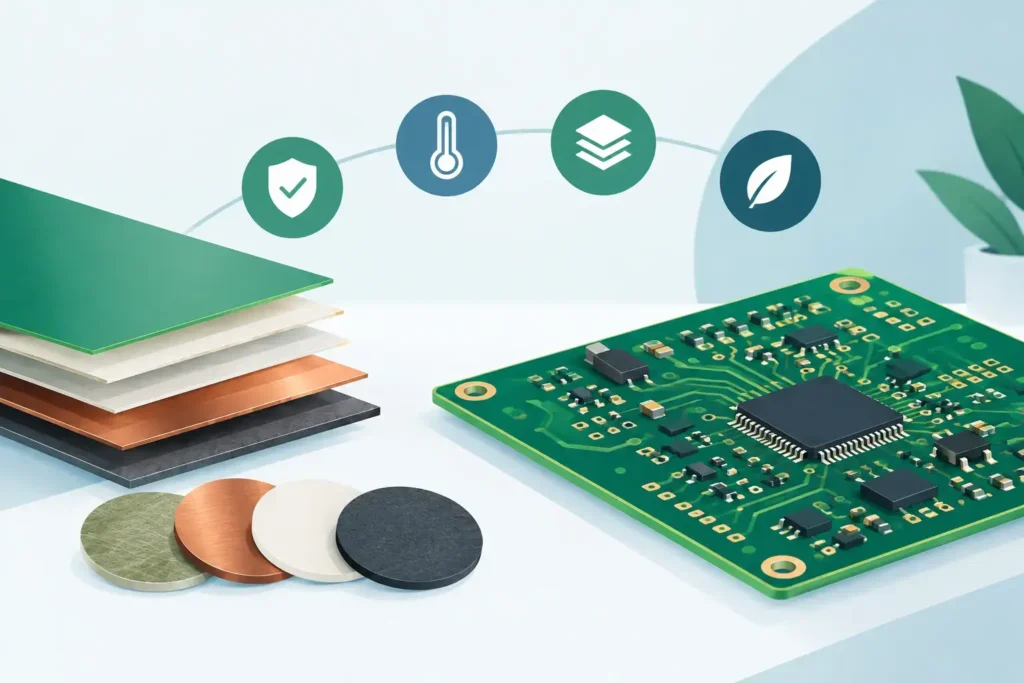
A high-frequency board rarely fails because a single trace was a few millimeters too long. More often, the failure occurs because the layer stackup was treated as a default setting with the PCB manufacturer. Therefore, how to choose a stackup for high-frequency PCBs must be decided before routing begins—not patched with additional ground vias after EMC measurements or once the first prototype displays unstable operation.
A stackup represents the electrical and mechanical contract between the schematic, layout, and manufacturing. It defines how signals reference their return paths, how return currents flow, how impedances are maintained, and how much coupling occurs between layers. For RF, high-speed digital interfaces, radar, data center infrastructure, and medical electronics, this is a design decision with direct consequences for signal integrity, power integrity, EMC, and manufacturing yield.
Start with the Actual Signal Requirements
The first question is not how many layers the board should have. It is which nets dictate the requirements for the stackup. A board containing a 2.4 GHz RF section, DDR4, Ethernet, and switch-mode power supplies presents multiple distinct sensitivities. They can coexist on the same PCB, but they must not be forced into the same compromise without an intentional plan.
For each critical signal group, determine the maximum frequency or edge rate, target impedance, allowable insertion loss, differential routing requirements, and layer transition constraints. Digital clock frequency alone is insufficient. A fast edge rate contains harmonics extending far beyond the fundamental frequency, imposing transmission line requirements even if the system seemingly operates at a modest data rate.
RF signals are further evaluated based on trace attenuation, adjacent coupling, via inductance, and the stability of the dielectric constant over frequency and temperature. A generic FR-4 material may suffice in some designs, whereas in others it introduces excessive variation or intolerable loss. The selection depends on frequency, link budget, trace length, temperature profile, and product lifecycle requirements.
Selecting a High-Frequency Stackup from the Reference Planes
A high-frequency signal requires a continuous, tightly coupled return path. Consequently, the stackup is best engineered from the inside out: begin with the plane pairs, and then place the signal layers relative to them. A signal layer placed in close proximity to a solid GND plane ensures controllable impedance, minimal loop inductance, and superior shielding from the rest of the board.
Simply having a ground plane somewhere in the stackup is insufficient. The dielectric distance between the signal and its reference plane is critical. Excessive spacing broadens field distribution, exacerbates coupling, and renders impedance more susceptible to process variations. Conversely, extremely tight spacing can impose tighter dielectric tolerances on the PCB fabricator and make specific impedance targets harder to achieve. The optimal spacing is therefore a carefully balanced decision, not an arbitrary rule to make everything as thin as possible.
On a multilayer board, high-speed signals should typically be paired with their own dedicated, adjacent reference plane. Routing on an internal stripline layer between two planes frequently delivers the best EMC performance because the electromagnetic fields are fully enclosed. An external microstrip layer may be appropriate for RF where access is required for tuning, testing, or specific coplanar waveguide geometries. However, it is more vulnerable to solder mask effects, component loading, enclosures, and environmental conditions.
Avoid Splits Under Critical Return Currents
A split GND or power plane beneath a high-speed signal forces the return current into a detour. The consequence can be increased radiation, reflections, and common-mode noise. If a signal must cross between reference planes, the transition must be engineered with appropriate stitching—typically GND vias located immediately adjacent to the signal via when both reference planes are ground.
If the signal shifts reference from GND to a power plane, the placement and high-frequency impedance of the PDN decoupling capacitors become part of the return path. While technically viable, this is rarely an acceptable baseline for critical nets. In demanding designs, maintaining an explicit, unbroken GND reference across the entire signal path is vastly preferable wherever possible.
Select Materials Based on Electrical Data, Not Just Tg
Tg is relevant for thermal reliability and assembly processes, but it does not characterize a laminate's suitability for high frequencies. For high-frequency designs, the primary evaluation criteria include Dk, Df, copper surface roughness, glass weave effects, material homogeneity, and the manufacturer's documented tolerances.
Dk governs impedance and propagation delay. Df determines dielectric loss, particularly as frequency and trace length increase. Copper roughness can substantially drive up insertion loss at high frequencies due to the skin effect concentrating current near the surface. Therefore, a low-loss laminate paired with the appropriate copper foil often delivers far greater value than simply specifying a high-Tg material.
This does not imply that every board necessitates an expensive RF laminate. Over-engineering drives up unit cost, restricts the supplier base, and introduces unnecessary manufacturing constraints. For many industrial applications, an engineered high-speed FR-4 system represents the optimal compromise. However, that compromise must be substantiated by simulated and documented losses, not the assumption that all FR-4 materials behave identically.
Specify Concrete Prepregs and Core Materials
A stackup must not merely state the layer order as signal, GND, and power. It must define exact core thicknesses, prepreg types, copper weights, and post-lamination impedance geometries. Prepreg flows during lamination, and the final dielectric thickness depends on copper distribution and the specific fabrication process.
When impedance tolerances are tight, the PCB manufacturer must provide a stackup with calculated trace widths and tolerances, approved prior to layout release. This approach is substantially more efficient than routing to nominal values and discovering later that the manufacturer's actual stackup necessitates revised trace geometries or spacings.
Co-Design Impedance, Vias, and HDI
Controlled impedance is not solely a function of trace width. It is governed by trace geometry, dielectric properties, copper thickness, solder mask, and reference plane spacing. Differential pairs simultaneously require strict control over intra-pair spacing, symmetry, via transitions, and surrounding copper. A pair can yield accurate results in a basic 2D cross-section calculation yet fail at BGA breakouts, AC coupling capacitors, or layer transitions.
Vias rapidly become the limiting factor as frequency rises. A through-hole via introduces stubs that can resonate and degrade signal integrity. Backdrilling, blind vias, or buried vias may be necessary, but they increase stackup complexity and manufacturing cost. This decision must be evaluated against the complete channel budget. There is no engineering value in implementing HDI if a properly dimensioned through-hole via satisfies the performance specifications.
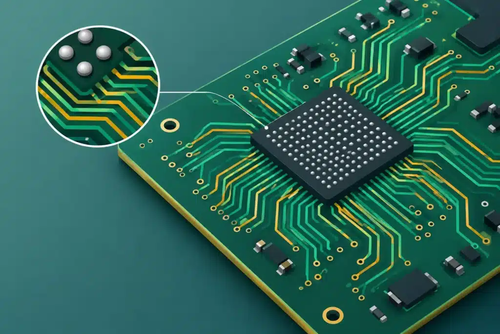
However, with dense, fine-pitch BGAs, HDI can be essential to preserve uninterrupted reference planes and eliminate problematic fanout topologies. That benefit frequently outweighs pure spatial savings by concurrently improving return paths, PDN performance, and overall routing discipline.
Integrate PDN and EMC from the Initial Layer Assignment
A stackup with well-managed signal impedances can still fail if the power distribution network is inadequate. Closely spaced power-GND plane pairs reduce plane loop inductance and support a low-impedance PDN at high frequencies. While they do not eliminate the need for discrete decoupling capacitors, they make those capacitors far more effective when component placement and via structures are executed properly.
Plane allocation must simultaneously account for current-carrying capacity, thermal dissipation, and voltage isolation. Thin copper layers are ideal for fine, impedance-controlled geometries, but may prove insufficient for motor loads, FPGA core rails, or thermal spreading. Frequently, an asymmetric functional stackup is required: fine-line signal layers adjacent to reference planes combined with heavier copper on dedicated power planes or outer layers.
Furthermore, EMC encompasses more than external enclosure shielding. A disciplined stackup confines electromagnetic fields, preventing them from coupling into external cables, chassis structures, and sensitive analog circuitry. This minimizes the need for downstream corrective measures such as added filtering, ferrite beads, or localized shielding cans.
Ensure the Stackup is Production-Ready Before Freezing Layout
The final stackup must be verified directly with the target PCB fabricator, rather than relying on theoretical generic profiles. The fabricator's stocked materials, press capabilities, minimum trace/space constraints, drill aspect ratios, and impedance tolerances must align fully with the design. IPC Class 3 projects, in particular, demand that electrical and manufacturing requirements are documented without ambiguity.
A comprehensive decision package consists of the detailed stackup drawing, material specifications, impedance table, critical routing rules, via stack architectures, and clearly defined requirements for impedance test coupons. If the design incorporates RF sections or high-speed serial links, full-channel and PDN simulations should be completed before the layout matures beyond the point of cost-effective architectural changes.
At Wise Choice Support, stackup design is treated as an integral component of the core PCB architecture—not a procurement document generated post-layout. This ensures a direct path from requirements to a production-ready PCB, eliminating discrepancies between prototypes and volume manufacturing.
The optimal stackup is not defined by the highest layer count or the most expensive laminate. It is the stackup in which every dielectric thickness, reference plane, material selection, and via structure is systematically justified by the actual signal, power, and manufacturing requirements. When that decision is established early, the remainder of the layout process becomes substantially more predictable.