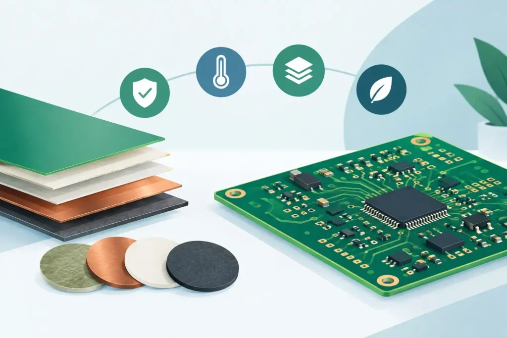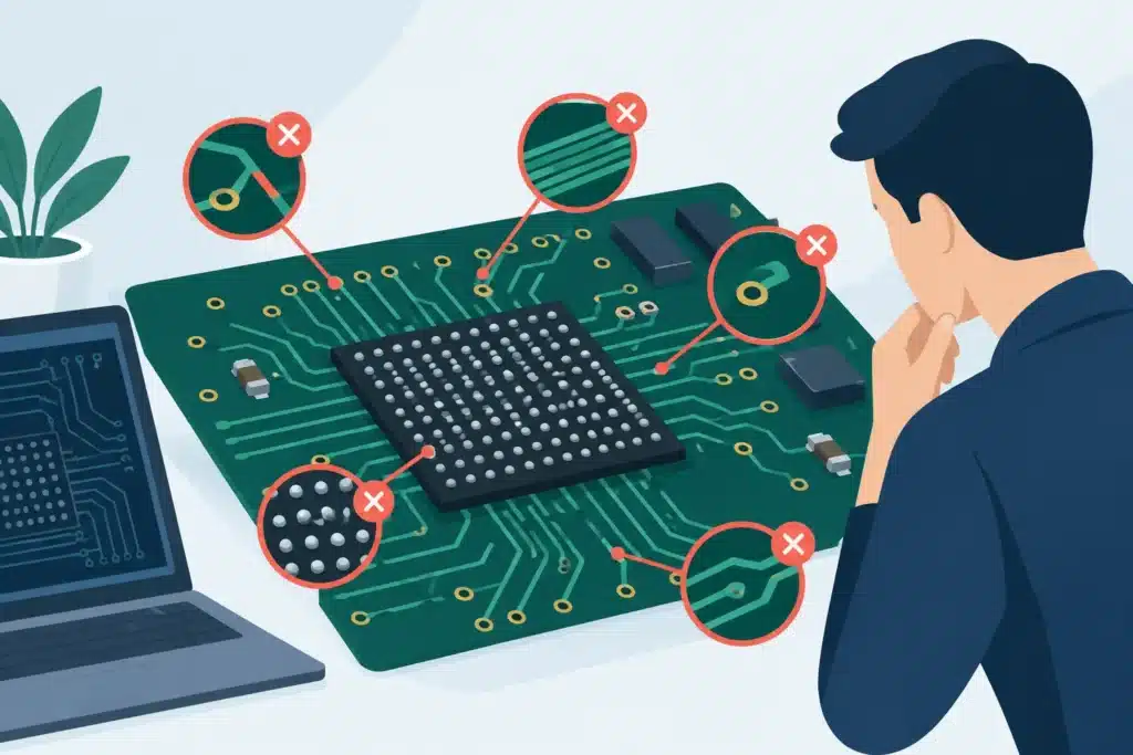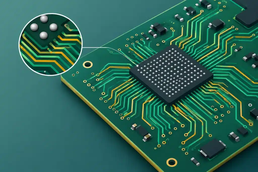
Material selection is often reduced to an item on the bill of materials: standard FR-4 or a more expensive laminate. This is a mistake. Selecting PCB materials is an integral part of the electrical, mechanical, and manufacturing engineering—and a decision that can determine whether the board passes EMC testing, maintains impedance, dissipates heat, and survives its expected service life.
A material is not merely a dielectric between two copper layers. Its dielectric properties, glass weave, resin content, thermal expansion, and compatibility with the fabrication process impact the entire design. In simple low-speed products, a well-documented standard laminate may be the right choice. In RF, high-speed, HDI, power electronics, medical technology, and mission-critical systems, however, the choice must be made based on concrete requirements—not habit or a generic stackup from the PCB fabricator.
Select PCB materials based on function, not material group
FR-4 is not a single, unambiguous material type. The designation covers a broad group of glass-reinforced epoxy laminates with vastly different properties. Two laminates, both termed FR-4, can diverge significantly in dissipation factor, dielectric constant, glass transition temperature, z-axis expansion, and stability across frequency and temperature.
Therefore, material selection should begin with the operational profile of the product. What frequencies and edge rates occur? What is the continuous and cyclic thermal stress? What are the requirements for operating life, humidity, vibration, vacuum, or chemical exposure? Are there fine-pitch BGAs, press-fit pins, heavy copper layers, or high-power-density components? Until these questions are answered, choosing between standard FR-4, high-Tg FR-4, low-loss epoxy, hydrocarbon ceramic, or polyimide is premature.
The optimal material is rarely the one with the most extreme datasheet figures. It is the material that delivers the necessary performance with a stackup, fabrication process, and supply chain that can be reliably replicated in series production.
Signal integrity: Dk and Df are only the beginning
In high-speed and RF designs, the dielectric constant (Dk) is critical to trace impedance and propagation velocity. The dissipation factor (Df) describes dielectric losses and grows in importance as frequency, trace length, or channel budgets increase. A material with excessive loss can reduce margin in a serial channel, degrade the eye diagram, or unnecessarily increase the need for equalization.
However, selecting based solely on a single Dk value from a datasheet is insufficient. The value depends on test method, frequency, resin content, and, in practice, the finished laminate construction. Prepreg after pressing does not necessarily exhibit the same properties as the specified core material. When impedance requirements are tight, the stackup must be calculated using actual thicknesses, copper weights, and material data from the selected fabricator.
The glass weave warrants equal attention. At high data rates, a differential pair can alternate between crossing glass bundles and resin-rich areas. This alters the local dielectric constant and can induce skew between the two conductors—known as glass weave skew. This issue cannot be mitigated through routing alone. The weave style of the material, trace geometry, routing angle relative to the weave, and layer allocation must be evaluated holistically.
Copper foil roughness is another parameter that is frequently overlooked. Rough copper increases losses at high frequencies because the skin effect forces current along a longer, more irregular path. Very smooth foil can improve channel insertion loss, but simultaneously demands that peel strength and fabrication processes remain tightly controlled. There is no universal rule here. A 28 Gbps link and an industrial controller with a 200 MHz bandwidth do not share the same requirements.
Controlled impedance must be manufacturable
An impedance calculation is only as valuable as its translation into a manufacturing requirement. Clearly specify target impedance, tolerances, reference planes, material family, copper thicknesses, and relevant test criteria in the fabrication data. It is also necessary to define ownership of any pre-production stackup adjustments.
If the fabricator alters the prepreg combination, resin content, or foil type without verifying impedance, it is no longer the design that was simulated. In critical projects, TDR coupons and potentially material certificates should be an integrated part of the quality requirements.
Thermal and mechanical characteristics govern operational life
A printed circuit board is subjected to mechanical stresses, even in static conditions. Temperature variations cause copper, resin, components, and solder joints to expand at different rates. The critical metric is often the CTE in the z-axis—through the thickness of the board. If expansion is excessive, vias, barrel plating, and solder joints can become overstressed during repeated thermal cycling.
Tg (glass transition temperature) is often used as a quick indicator, but high Tg alone does not guarantee reliability. Decomposition temperature (Td), thermal stress resistance, time-to-delamination, and z-axis CTE are equally critical. For multilayer boards with high layer counts, large BGAs, or significant thermal cycling, the material must be evaluated against the specific mission profile—not merely against maximum ambient temperature.
A high copper balance aids in thermal distribution, but also alters lamination dynamics, resin flow, and the mechanical assembly. Effective cooling solutions employing thermal vias, copper balance, metal enclosures, or heat spreaders therefore require a comprehensive thermal analysis. A material with higher thermal conductivity may be beneficial, but it cannot compensate for a layout that lacks a physical conduction path out of the board.
In aerospace, defense, and other environments subject to extreme temperature swings, moisture absorption and outgassing can also be decisive. In these applications, documentation, lot traceability, and material suitability must be treated as baseline design constraints from the outset.
HDI and fine pitch impose different laminate requirements
HDI boards with laser microvias, sequential lamination, and fine-pitch BGAs cannot simply be manufactured like standard multilayers with higher layer counts. The material must withstand multiple lamination cycles stably and support reliable laser drilling, desmear, metallization, and via filling.
Resin content and glass weave influence both laser processing and dielectric thickness. An extremely thin dielectric may be required for via aspect ratios or power integrity, but it imposes stringent demands on process control and dielectric breakdown strength. Simultaneously, the transitions between build-up layers, buried vias, and through-hole vias must be engineered for reliability, not merely routability.
Material selection also governs the risk of Conductive Anodic Filament (CAF) formation. Under humidity and electrical bias, unwanted conductive pathways can form along the glass-resin interfaces. This risk increases with higher voltages, tight via geometries, moisture, and mechanical stress. In products with extended lifecycle requirements, spacing, hole-wall quality, material datasheets, and CAF resistance ratings must be evaluated explicitly.
EMC, PDN, and materials are inextricably linked
A PCB material does not resolve EMC issues on its own, but it defines the physical parameters within which the layout must operate. Thin dielectrics between power and ground reduce plane inductance and improve the high-frequency performance of the PDN. This can lower supply rail noise and establish better operating conditions for high-speed digital circuitry.
Concurrently, this demands precise control over stackup architecture and resonances. Adding more plane pairs is not inherently beneficial if the layer distribution causes unforeseen impedance discontinuities or complicates return current paths. The material's Dk, layer thicknesses, and copper distribution map directly into the electromagnetic geometry.
For RF applications, stability over temperature and frequency is often more vital than a nominally low Dk. Antennas, filters, and controlled transmission lines react to even slight substrate variations. If a frequency-critical function is routed on a mixed-material board, the transitions between materials and reference planes must be modeled and analyzed, not assumed ideal.
Manufacturability, availability, and documentation drive the decision
An exotic laminate may be technically compliant yet prove to be a poor project choice if few fabricators can process it, lead times are unpredictable, or second-source alternatives cannot be qualified. Material selection should always occur in coordination with the fabricator intended to produce the board—particularly when IPC Class 2 or Class 3, tight impedance tolerances, HDI, or specialized surface finishes are required.
Material callouts on drawings must be unambiguous. Define the material family or approved equivalents, Tg and Df specifications, copper foil type, layer stackup, and requirements for certifications and testing. A vague callout such as "high-Tg FR-4" leaves wide latitude to the manufacturer and may necessitate costly re-qualification later.
Cost must also be viewed holistically. Lower raw laminate costs can become expensive if they lead to additional EMC iterations, lower manufacturing yields, difficult assembly, or field failures. Conversely, low-loss materials offer no business value in a design that faces neither loss nor stability constraints. Wise Choice Support therefore evaluates material selection in direct conjunction with layout, stackup design, simulation, and manufacturing requirements—not as an isolated purchasing decision.
The most effective time to select materials is before the layout is locked. By translating signal integrity, PDN, thermal, and manufacturing requirements into a verified stackup early, the engineering team secures a printed circuit board that is not only manufacturable, but built to operate reliably throughout the product's operational life.